
Lecture
Based on an analysis of the world literature, this paper presents the main methods for producing metamaterials for the optical range, in particular 3D photonic metamaterials. It examines the prospects of individual technologies and the issues of establishing large-scale production and reducing its cost.
Recently, considerable attention has been given to research and development of so-called metamaterials, on the basis of which fundamentally new devices for radio electronics and photonics are expected to be built: devices with negative refraction for controlling radiation in the terahertz and visible wave ranges, frequency multipliers and amplifiers, superlenses for obtaining sharp images of very small elements without diffraction distortion, small but highly directional antennas, coatings for electromagnetic cloaking, and much more .
The term “metamaterial” denotes the transformation of an ordinary homogeneous material into a more complex “super-material” by assembling it from a huge number of miniature modules called “meta-atoms”. The latter are not atomic particles in the usual sense, but they are composed of them and are made of metals and dielectrics. The number of meta-atoms even in a small piece of metamaterial
reaches 106-109
.
Meta-atoms are tiny elements made of short lengths of wire, strips, plates, rings, spirals, or spheres; they can also take the form of a flat lattice with holes, and so on. As the operating frequency increases – from gigahertz to terahertz and hundreds of terahertz – that is, up to frequencies of the optical range, the size of the meta-atoms has to be reduced, moving from bulk microelements to nanofilms and nanocoatings. In doing so, the configuration of the meta-atoms ensures
that they perform the functions of the simplest electrical (radio) components – capacitors, inductors, oscillating circuits, or resonators. Metamaterials can also be regarded as composites whose heterogeneous medium contains inclusions, but unlike other types of composite material, these inclusions are themselves electrical (radio) components.
Owing to inclusions of this kind, metamaterials possess unique electrical (radio), physical, and optical properties resulting from resonant interaction with the electromagnetic field. In particular, metamaterials can exhibit negative permittivity and permeability, and the phase and group velocities of an electromagnetic wave can point in opposite directions, leading to negative refraction. Repeated local field enhancement in the region of a resonating meta-atom makes it possible to realize various nonlinear effects . Thus, the concept of a “metamaterial” also implies possessing properties unavailable to the ordinary materials from which the meta-atoms are made, or, at the very least, that the properties of the metamaterial exceed those of the meta-atom material itself, for example in multifunctionality. This review examines technologies for producing metamaterials capable of operating in the optical wave range, including several promising methods for realizing 3D photonic metamaterials.
For true metamaterials, the meta-atom size must be much smaller than the
electromagnetic wavelength, so that the wave “does not see” the individual meta-atoms, by analogy with the way
a light wave “does not see” the individual atoms of an ordinary material. In this case the metamaterial can be treated as a continuous
homogeneous medium rather than as an integrated circuit,
in which the wave interacts with each of its elements independently, in sequence. Let us give some estimates of the ratio between the wavelength
and the size of the structural elements of various materials.
In an ordinary crystal, the atoms are arranged
periodically with a lattice period (constant) of about half a
nanometre. This value is smaller by several
orders of magnitude than the wavelength of visible light, and even more so than
the wavelengths of the terahertz and gigahertz ranges.
For example, the wavelength of green light is approximately 500 nm, while the wavelength for
optical communication at a frequency of 200 THz is 1.5 µm; therefore, for this direction
of propagation the light wave “sees” an essentially homogeneous medium, i.e., it “does not see”
the underlying periodicity, only the basic
symmetries of the crystal. Hence, for visible
light and the near-IR range, the meta-atom size must not exceed 50-100 nm, and
nanotechnology is required here! For centimetre waves, the meta-atom size can be
larger – up to several millimetres – and here
printed-circuit-board technology is used.
As a result, a metamaterial can be characterized by various parameters applicable to a continuous medium, for example, reflection, transmission, and absorption coefficients, permittivity and permeability
, and the refractive index.
The first photonic metamaterials were
created on the basis of ultra-miniature LC resonant circuits borrowed from
microwave metamaterial technology, in particular, split-ring
resonators, made from
printed-circuit-board foil . For frequencies on the order of
hundreds of terahertz, these resonators have the configuration shown in Fig. 1a. Here the function
of the inductor (its dimensions are 380 nm×430 nm) is performed by an open flat loop made of a metal film 80 nm wide; the function of the capacitor is performed by the gap at the point where the loop is broken. Gold is normally used as the loop material.
To raise the operating frequency, the
values of inductance and capacitance must be
reduced. For this purpose the “loop” is made from two gold
nanostrips (segments of nanorods or nanowires, see Fig. 1b), which play the role
of the inductor. The end sections of the nanostrips
form two capacitors connected in series. In Fig. 1b the arrows show
how the current flows in the nano-LC circuit (nanoresonator). On the right of the same figure
the metamaterial is shown schematically as a lattice of
paired metal nanostrips. It is clear
that a dielectric material must be placed between the strips
for mechanical fixing. Fig. 1c shows a
top view of fabricated samples of a single
nanoresonator (left) and a lattice of them (right); the resonant frequency is about 200 THz and above (λ ≤ 2 µm) . The nanoresonator is fabricated as
a film structure Au(50nm) –
SiO2(50nm) – Au(50nm).
Fig. 1b shows the orientation of the vectors
(polarization) of the electromagnetic field of the incident light; here k is the wave vector. It is clear that for the light to interact effectively with the metamaterial lattice, the magnetic field vector H must be directed normal to the plane of the loop.
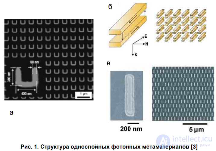
Fig. 1. Structure of single-layer photonic metamaterials
In this case, the
current induced in the loop, and the loop's
own magnetic field directed against the magnetic field of the light wave, will be maximal.
With this polarization, the light must fall
normal to the plane of the lattice, which makes it easier to
fabricate it for use with a wide light
beam.
In the case of split-ring
resonators arranged in a plane (Fig. 1a),
the situation is different: the vector H should preferably be directed normal to the plane of the lattice, with the light
passed along it. When working with a wide
light beam, it becomes necessary to switch to multilayer lattices (3D metamaterials), whose overall
thickness must match the width of the light beam – this leads to serious technological problems.
To reduce the dependence on the azimuthal direction of the light polarization (the direction of vector H), the strips of the nanoresonators are replaced with round nanodiscs, hexagonal,
or, at the very least, square nanoplates, as, for example, in Fig. 2a , where the nanoresonators take the form of multilayer “tablets”:
Au(20nm) – MgF2(60nm) – Au(20nm). The metamaterial can also be made as a multilayer structure with holes, as in Fig. 2b
{Au(30nm) – Al2O3(75nm) – Au(30nm)}, which
provided a negative real part of the refractive index Re(n) ≈ –4 at a wavelength of 1.8 µm .
A substantial reduction in losses, i.e., high metamaterial quality, was achieved in a
sheet structure of the “fishnet” type with rectangular holes and silver conductors (Fig. 2c,d), where ax = ay = 600 nm,
wx = 316 nm, wy = 100 nm, t = 45 nm, s = 30 nm .
For the polarization shown in Fig. 2c, the paired ax strips served as the inductive element, and the ay strips – as the capacitive one. For this
structure a negative refractive index Re(n) ≈ –2 was obtained at a wavelength
of about 1.45 µm.
To obtain a 3D metamaterial, it is built up along the third coordinate, as shown schematically in Fig. 1b (view on the right). In
practice this can be achieved by stacking
sheets or layers of the 2D material, using
planarization and pattern-alignment techniques, along with other approaches
established in modern microelectronic
technology. Fig. 3 shows a four-layer
metamaterial based on split-ring resonators, each layer of which is obtained by depositing metal by vacuum
evaporation, then depositing a resist, exposing it by electron-beam irradiation, and developing the resist to form a mask; this is followed by ion-beam etching of the metal and planarization of the resulting lattice (the permissible roughness of the planarized surface must not exceed 5 nm).
The next
layer is then deposited and processed, with the alignment procedure carried out.
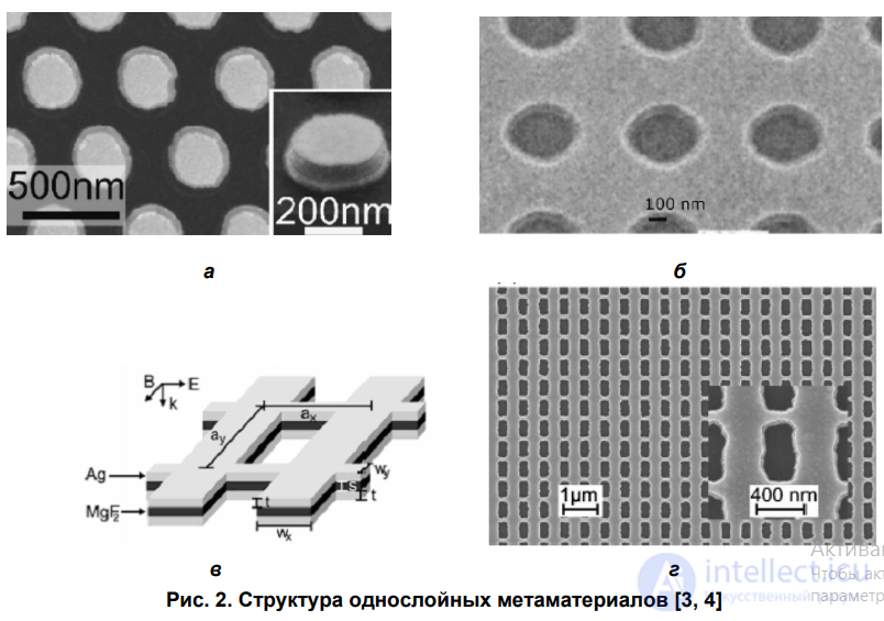
Fig. 2. Structure of single-layer metamaterials [3, 4]
Because of the problems associated with the accumulation
of errors during repeated alignment of the patterns of individual layers, the number of layers is limited (so far, no more than 20).
Fig. 4 shows a fragment of a material
with multilayer tablet-type meta-atoms.
A 3D meta-atom takes the form of a multilayer pyramid (prism) or cone (cylinder) and represents a further development of the three-layer
tablet shown in Fig. 2a.
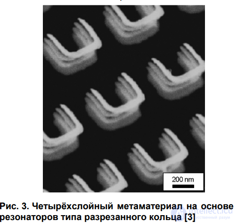
Fig. 3. Four-layer metamaterial based on
split-ring resonators
Metamaterials of this kind can be produced
in various ways. Fig. 5
shows two process schemes using multilayer deposition of metal/dielectric combined with explosive lithography (a) or deep anisotropic etching (b) for
forming the geometry of the meta-atoms.
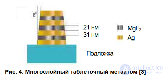
Fig. 4. Multilayer tablet-type meta-atom
There are reports in the world literature
of other methods used to obtain
3D metamaterials: two-photon photopolymerization based on nonlinear photonic processes, chemical reactions for direct pattern formation with local exposure
to a focused electron, ion, or
laser beam, interference lithography, and mechanical “nanostamping” of polymer films, including resist films, and metal films (the nanostamping method is known as “nanoimprint lithography”). Attempts have been made to organize self-assembly processes
for metamaterials, as has already been achieved for photonic crystals.
Two-photon photopolymerization occurs at the focal point of a laser beam, where simultaneous absorption of two photons is possible. By scanning space with the focal point,
a polymer structure of complex shape can be formed within it. A thin silver film can then be deposited onto the resulting three-dimensional structure by a chemical
or electrochemical method.
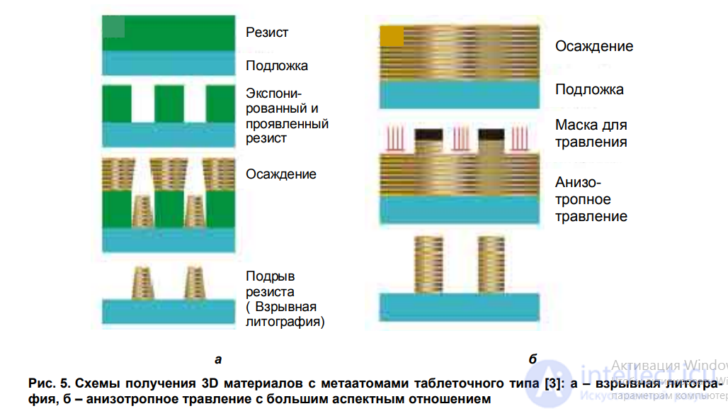
Fig. 5. Schemes for obtaining 3D materials with tablet-type meta-atoms : a – explosive lithography, b – high-aspect-ratio anisotropic etching
It is possible to apply a low-temperature method of chemical vapour deposition from
vapours of organometallic compounds (the
CVD method). This makes it possible to obtain polymer
structures with a continuous metal film
or structures in the form of isolated polymer objects. For the latter, a selective metal deposition method is used, based on
choosing the polymer and the type of its treatment. Fig. 6
shows a 3D metamaterial consisting of more than 700 microstructures obtained by this method.
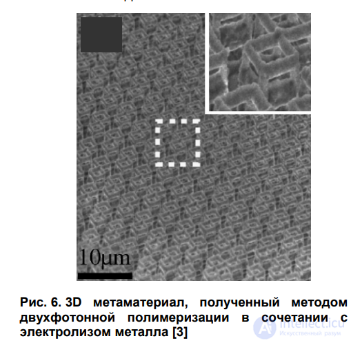
Fig. 6. 3D metamaterial obtained by two-photon polymerization combined with metal electrodeposition
Fig. 7 shows a fragment of a 3D metamaterial obtained by direct laser
writing . It can be seen that this metamaterial consists of vertical chains of split-ring resonators; the resonators of the chains are arranged in two planes, so
this metamaterial has a negative
refractive index for two directions of
light transmission.
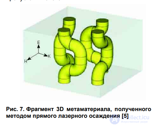
Fig. 7. Fragment of a 3D metamaterial obtained by direct laser writing
From the information presented above, it follows that photonic metamaterial technology must be based on processing methods
with nanometre-scale resolution. Here
electron-beam lithography and focused-ion-beam milling play an important role, but since these methods process surface elements sequentially, they are characterized by low throughput and high cost, and are suitable
only for producing laboratory samples, as well as templates, masks, and nanostamps.
Deep anisotropic etching using a mask and a wide directional ion-plasma flow (Fig. 5b) solves
this problem to some extent, but problems remain with a fast method for forming the mask pattern and
their resistance to sputtering.
Methods of direct structure formation using electron, ion, and laser
beams to initiate local reactions
are characterized by sequential processing
of elements, so they likewise fail to provide
the required throughput.
Relatively high throughput
in pattern formation is provided by interference and nanoimprint lithography, in
which all surface elements are processed in
parallel. These lithography methods combine well
with the multilayer-material processing technologies shown in
Fig. 5.
A promising approach is the combination of two-photon polymerization with interference lithography, in which elements of the 3D structure are created simultaneously at
many points in space (where the light field
of the interference pattern has high
intensity). But this method, like the others, requires
considerable further development.
The material and quality of the conducting layers are of great importance, since a key point in obtaining functional photonic
metamaterials is ensuring low losses;
in particular, it is necessary to minimize the resistance of metal films tens of
nanometres thick. To do this, it is necessary to ensure
their continuity, reduce roughness, and increase resistance to environmental exposure. At present, conducting films are made
mainly from silver and gold; the former
has lower resistance but is sensitive to environmental exposure. It is also important
to ensure low roughness of the dielectric layers (substrates) onto which the
Nanostructures and nanotechnologies in electronics 55
metal is deposited. SiO2,
MgF2, or Al2O3 are used as inorganic dielectric materials.
Among the deposition methods for flat substrates,
vacuum electron-beam evaporation methods predominate. The authors of this paper are currently studying the use of
the pulsed magnetron sputtering method
for depositing both conducting and dielectric layers of the required quality in a single
process cycle. This method provides enhanced energetic activation
of the condensation process and makes it possible to deposit
material with increased density and low
roughness . Chemical deposition methods for metals from solutions of their chemical
compounds, and CVD, also have a certain
potential, especially in the case of substrates of complex shape.
In conclusion, we note that not very
much time has passed since the start of intensive
research into photonic metamaterials, but
substantial useful results have already been achieved, and success in the field of technology gives
hope for their practical application, although
there is still a great deal of work ahead.
[[b8211]]

Comments