Lecture
Это окончание невероятной информации про схемотехника комбинационных узлов.
...
элементом ИЛИ. Такое построение КС обеспечивает ее максимальное быстродействие, так как ранг схемы минимален. Однако, не всегда возможно на первом уровне и, особенно, на втором выбрать логические элементы с требуемым К об , т.к. может оказаться, что ЛЭ с таким К об не выпускаются промышленностью. В этом случае необходимо с помощью нескольких элементов с меньшим К об получить эквивалент с большим К об либо, что предпочтительней, преобразовать БФ, перейдя от ДНФ к скобочной форме. Этот переход сопровождается уменьшением К об логических элементов, требуемого для построения схемы. Осуществить такой переход можно с помощью факторного алгоритма , суть которого рассмотрим на примере.
Пусть задана некоторая булева функция в виде:

Для реализации этой функции по приведенному выражению необходимо использовать 3 логических элемента 4И, один логический элемент 5И и один логический элемент 4ИЛИ.
С помощью факторного алгоритма получим скобочную форму для заданной функции. Для этого обозначим все конъюнкции буквами:


 ,
, 
и будем рассматривать их как некоторые множества. Находим попарные пересечения множеств:
 ,
,  ,
,  ,
,  ,
,  ,
,  .
.
Полученные пересечения показывают общие части отдельных конъюнкций. Выбираем пересечение, которое имеет наибольшую длину (если такое отсутствует, то выбирают то, которое чаще всего встречается). В данном случае это  . Поэтому из конъюнкций А и В выносим общую часть
  . Then we have:
 .
.
Обозначим F =  и находим пересечения:
 ,
,  ,
,
Следовательно, для исходной функции имеем:
 .
.
Denote  ,
,
Пересечение  . Следовательно, окончательно имеем:

Для реализации функции по последнему выражению необходимо 5 элементов 2И, 1 элемент 3И и 3 элемента 2ИЛИ (рис. 3.30).
 |
Fig. 3.30 Функциональная схема, полученная на основании
факторного алгоритма
Как видно из полученной схемы, для ее реализации необходимы элементы с К об = 2 или 3 (в отличие от исходной схемы с К об = 4 или 5). Однако ранг схемы увеличился до 7, что приводит к увеличению задержки срабатывания схемы.
На такой параметр, как быстродействие проектируемой схемы оказывает существенное влияние два фактора: задержка , вносимая каждым элементом ИС , участвующим в функционировании этой схемы и количество последовательно подключенных таких элементов в цепи формирования выходного сигнала. Если существует несколько параллельно соединенных последовательных цепей, участвующих в формировании выходного сигнала, то быстродействие схемы вычисляется по значению задержки той последовательной цепочке, которая вносит максимальную задержку. Помимо этого, на быстродействие цифровой схемы определяется еще и задержками в цепях соединений между ИС, входящими в проектируемую схему. Значение этих задержек зависит от длины проводников, их взаимного расположения и расстояния между ними. С учетом того, что эти параметры определяются на этапе разработки монтажной схемы и изготовления устройства, и, если предполагается эксплуатация разрабатываемого устройства на частотах, близких к максимально допустимым, необходимо на этих этапах разработки принимать необходимые меры по минимизации такого типа задержек.
Помехоустойчивость – это параметр, определяющий уровень значений импульсных помех , возникающих в цепях ЦУ питания в процессе его работы.
Типовой проблемой в данном случае является, в частности, наличие токовых импульсов в цепях питания ИС, которые создаются сквозными токами выходных каскадов типа и токами перезаряда емкостей.
Импульс сквозного тока переключающего ЛЭ1 (рис. 3.31,а) I СКВ протекает через транзисторы выходного каскада, условно изображенные замкнутыми ключами, от источника питания U CC на общую точку схемы GND через линии, имеющие полные сопротивления Z CC и Z GND . Главную часть сопротивлений составляют индуктивности линий, на которых выделяются напряжения U L =Ldi/dt . Протекание сквозного тока создает на линии питания отрицательный импульс, а на линии общей точки («земли») – положительный.
Эти импульсы воздействуют на подключенный вблизи элемента ЛЭ1 элемент ЛЭ2 . Если, как показано на рисунке, ЛЭ2 находится в состоянии лог. «0», то его выход через насыщенный транзистор выходного каскада, отображаемый замкнутым ключом, связан с линией GND , следовательно, импульс с этой линии попадает на выход ЛЭ2 . При единичном состоянии элемента ЛЭ2 на его выход пройдет отрицательный импульс помехи с линии источника питания.
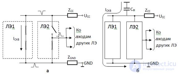
Fig. 3.31. Схемы, поясняющие процесс возникновения импульсных помех при переключении ЦЭ (а), и пути протекания сквозного тока при наличии в схеме фильтрующего конденсатора (б)
Для борьбы с этими опасными помехами нужны «хорошая земля» и фильтрация напряжения питания. Качество «земли» улучшается конструктивными мерами, снижающими сопротивление Z GND : шины «земли» делают утолщенными, нередко для их реализации на печатных платах отводят целые плоскости многослойных конструкций, систему заземления соединяют с несколькими выводами на входных разъемах, чтобы сократить пути прохождения токов в этой системе и уменьшить активное сопротивление на контактах разъемов.
Для шин питания схемы наряду с конструктивными методами борьбы с помехой применяют и схемотехнические:
- в цепи выходных каскадов добавляют небольшие сопротивления, ограничивающие сквозные токи и токи перезаряда емкостей,
- используют элементы с управляемой крутизной фронтов для уменьшения производных сигнальных напряжений и токов,
- применяют развязывающие каскады на выходах ИС для ограничения емкостных нагрузок на этих выходах,
- используют фильтрацию питающих напряжений.
Для фильтрации напряжений питания между линией U CC и «землей» включают конденсаторы. Высокая эффективность этого метода борьбы с паразитными связями элементов через цепи питания связана со следующим обстоятельством. ЦУ питаются от высококачественных источников стабилизированного питания, внутреннее сопротивление которых достаточно мало. Однако цепи обратной связи этих источников инерционны и не успевают отрабатывать короткие импульсы помехи. Поэтому для коротких помех выходное сопротивление источника питания не обеспечивает того низкого уровня, которое оно имеет при статическом режиме работы ЦУ. Установка фильтрующих конденсаторов С Ф создает путь (рис. 3.31,б), по которому замыкаются импульсы сквозного тока и токи перезарядки емкостей, минуя сопротивление U CC . Естественно, конденсаторы должны иметь малое сопротивление для высокочастотных сигналов, поэтому для фильтрации выбирают те типы конденсаторов, которые имеют малые паразитные индуктивности. Рекомендации по числу, типу и емкости фильтрующих конденсаторов вырабатываются практикой и приводятся в руководящих материалах по применению конкретных типов ИС.
 В завершении рассмотрения проблем борьбы с помехами следует сказать, что на практике диапазон допустимых значений этих помех находится в диапазоне 0,6-0,9 В.
The value of power dissipation or power consumption of the IC and other elements of the designed CU need to know in order to formulate the requirements for power supplies and design of heat sinks. The use of heat sinks is necessary in cases where its natural selection is not enough to absorb the power dissipated by the elements of the device circuit. It must be remembered that the total power dissipation consists of static and dynamic components. And, if the value of the static power can be obtained from reference data on the elements used in the scheme, then the value of the dynamic power, i.e. the power consumed by the elements in the process of switching them from one state to another can be recognized only by calculation. It should be understood that the main parameter that determines the level of dynamic power is the clock frequency of the control unit.
Taking into account the fact that in the formulation of a synthesis problem or in the process of an abstract KU synthesis, digital elements with an open collector (drain), an open emitter (source) or output having a third state (high impedance) can be selected as basic elements at the stage development of schematic diagrams of such devices must take into account the peculiarities of the connection of the inputs and outputs of these elements, as well as their connection to the power circuits In addition, in the developed CG, it is necessary to provide a circuit solution for controlling the output of signals from these elements in order to prevent simultaneous output of signals from several circuit elements to the same line.
To prevent simultaneous output of signals to the output line from several elements having a third state , such elements are provided with a control signal, usually called an Output Enable. With permission (OE = 1), the element works as usual, performing its function, and if it is not (OE = 0), it goes into the “disabled” state. The outputs of such elements can be connected in parallel, i.e. connect to one line, provided that at any time only one of them can be active. In this case, the disabled outputs do not prevent the active from generating signals at the connection point of the outputs. Such elements require the mandatory observance of the condition ОЕ 1 + ОЕ 2 + ... + ОЕ n ≤1 when connecting n outputs. Violation of this condition can even lead to failure of the elements themselves.
In the case of using open collector elements (drain), to form a high level of output voltage when locking the output transistor of such an element, it is required to connect external resistors connected to a power source. The resistance value of these resistors depends on the number of elements connected to the same output. This circumstance allows to increase the load capacity of the element with OK compared to conventional LEs. It should be understood that the high resistance of the load resistors leads to a decrease in the performance of elements with OK. Finally, the resistance value of the load resistor is selected taking into account the speed of the circuit and the power it consumes. In addition, if the outputs of several elements with OK are connected in parallel, you can implement either additional mounting logic or parallel operation of elements with OK on one output line, in the same way as it is done on vehicle elements. In this case, one of the usual element inputs can be used as a signal of the OE for the elements of the vehicle in elements with OK. If we are talking about the element NAND, then submitting a log. "0" on any of the inputs, you can prohibit the operation of this element by setting its output to the open state, regardless of the state of other inputs.
The problem of designing digital devices, including the COP, and the question of the criteria for their quality. Since the same problem can be solved in many ways, there are alternative project options that need to be able to compare with each other. The objective complexity of the comparative evaluation of options is due to the fact that a set of properties for each option matter — particular criteria of its quality. Each particular criterion has a clear, definite meaning (hardware complexity, speed, power consumption, noise immunity, etc.), but cannot exhaustively characterize the variant. To take into account several partial quality criteria, it is necessary to form a general criterion (integral, multi-purpose, quality function, value function). The formation of such a criterion is an extremely important task that has no formal solution. In any form of the general criterion includes factors assigned subjectively. Thus, a situation arises when a criterion is used to evaluate a device, but for it the quality assessment itself does not exist. Therefore, in practice, the design of complex overall quality assessment criteria are not popular. The most recognized criterion is the complexity-speed .
The complexity of the circuit is estimated by the amount of equipment making up the circuit. When designing circuits based on a specific element base, the amount of equipment is usually measured by the number of packages (modules) of integrated circuits used in the circuit. In theoretical developments, they are oriented towards an arbitrary element base and, therefore, to assess the costs of equipment, the estimation of the complexity of the Quine schemes is used.
The complexity (price) of Quine is determined by the total number of inputs of logic elements in the circuit.
With such an assessment, the unit of complexity is one input of a logical element. The price of the inverse entry is usually taken equal to two. This approach to the assessment of complexity is justified for the following reasons:
- the complexity of the scheme is easily calculated by Boolean functions, on the basis of which the scheme is built: for a DNF, the complexity of the scheme is equal to the sum of the number of letters (the letter with the negation sign corresponds to price 2) and the number of disjunction characters increased by 1 for each disjunctive expression.
- all the classical methods of minimizing Boolean functions ensure the minimality of the scheme in the sense of the Quayne price.
Practice shows that the scheme with the minimum price for Quine is usually implemented by the smallest number of structural elements - integrated circuit packages.
The speed of the combinational circuit is estimated by the maximum signal delay when it passes from the circuit input to the output, i.e. determined by the time interval from the moment of receipt of input signals until the establishment of the corresponding output values The signal delay is a multiple of the number of elements through which the signal passes from the input to the output of the circuit. Therefore, the speed of the circuit is characterized by the value of rt , where t is the signal delay on one element. The value of r is determined by the number of levels of the combinational circuit, which is calculated as follows. The inputs of the COP is attributed level 0 . Logic elements associated only with the inputs of the circuit refer to level 1 . An element refers to level k , if it is connected by inputs to elements of levels k -1 , k -2 , and so on. The maximum level of r elements determines the number of CS levels, called the rank of the scheme . An example of determining the rank of the r scheme is shown in Figure 3.32.
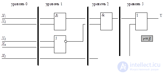 |
Fig. 3.32 Determining the rank of a circuit
Thus, after obtaining as a result of the synthesis several variants of the technical implementation of the CS and an assessment of the quality of the implementation of each of the options, the final decision is made to choose the variant of the scheme that has the minimum complexity coefficient (minimum price) and the maximum speed.
1. What is meant by combinational nodes.
2. What is the truth table used for?
3. What are the simplest combinational nodes, implemented in the form of chips?
4. Give the definition of the encoder and how it differs from the priority encoder.
5. Give the definition of the decoder and how it differs from the code converter.
6. In what form the Boolean function should be presented for its implementation on the basis of a decoder.
7. Give the definition of a multiplexer and give an example of a truth table for it.
8. Give the definition of a demultiplexer and give an example of a truth table for it.
9. The main purpose of the tire formers.
10. Draw a conditional graphic symbol of a four-digit comparator with three outputs and describe the purpose of all inputs and outputs.
11. What is the difference between serial adders and parallel adders?
12. How to produce a subtraction using an adder.
13. Draw a conditional graphic ALU and describe the purpose of all inputs and outputs.
14. List the problems solved at the stage of abstract synthesis.
15. List the problems solved at the stage of circuit synthesis.
16. List the main factors that should be taken into account when building a schematic diagram.
17. Explain the process of occurrence of impulse noise when switching digital elements.
18. List the main constructive measures to combat interference in digital devices.
19. Criteria for assessing the quality of technical implementation of combinational circuits.
Часть 1 Theme 3. Circuit design combinational nodes
Часть 2 3.7. Компараторы - Theme 3. Circuit design combinational nodes
Часть 3 3.11.2.5 Быстродействие - Theme 3. Circuit design combinational nodes

Comments
To leave a comment
Computer circuitry and computer architecture
Terms: Computer circuitry and computer architecture