Lecture
A key feature of modern FPGAs is that they contain special logic and internal connections necessary to implement accelerated transfer schemes. This logic is complemented by special internal connections between logical cells within each section, between sections within each LPR, and between LLDs.
Special fast transfer logic and dedicated routing facilitate logical functions such as counters, adders, and the like. The capabilities of accelerated transfer schemes in conjunction with the capabilities of other tools similar to shift registers based on correspondence tables, embedded multipliers and other blocks provide the necessary set of tools for using FPGAs in digital signal processing (DSP) applications.
In the process of implementing most applications, it becomes necessary to use memory cells, so modern FPGAs contain fairly large blocks of internal memory, called blocks of embedded RAM. Depending on the architecture of the chip, these blocks can be located around the perimeter of the crystal, scattered around its surface and relatively isolated from each other or arranged in columns, as shown in Fig.8.1.
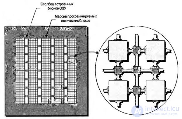
Fig.8.1. View on FPGA crystal with columns of built-in RAM blocks
Depending on the device, the size of the RAM blocks can vary from a few thousand to a few tens of thousands of bits. Each chip can contain from several lines to several hundred of such blocks. Thus, the total capacity extends from several hundred thousand bits to several million bits.
Each block of RAM can be used either as an independent storage device, or be in conjunction with several blocks to implement large-capacity memory arrays. Blocks can be used for various purposes, for example, as standard single-port and dual-port RAM, FIFO queues (first-in first-out — first came, first out), finite state machines, and so on.
Some types of functions, such as multipliers, are inherently rather slow when implemented using a large number of programmable logic blocks connected together. Since these blocks are used in numerous applications, many FPGAs contain special hardware multiplication blocks. These blocks are usually located in close proximity to the built-in RAM blocks, since they are often used together (Fig. 8.2).
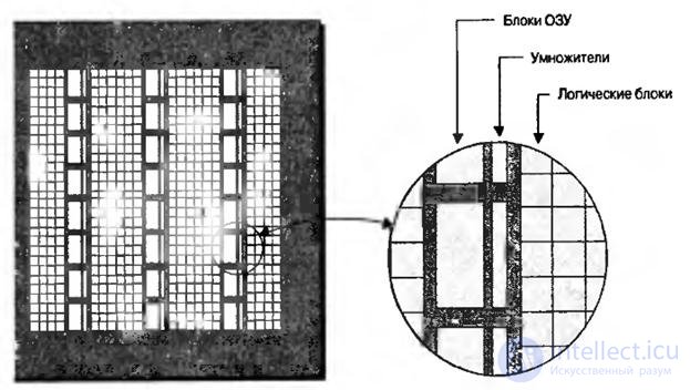
Fig.8.2. Crystal view with columns of built-in multipliers and RAM blocks
Some FPGA manufacturers also offer dedicated totalizers. At the same time, one of the most common operations used in digital signal processing applications is multiplication with accumulation (multiply-and-accumulate or MAC), Fig. 8.3. As the name suggests, this function multiplies two numbers and summarizes the result with the current number stored in the battery.
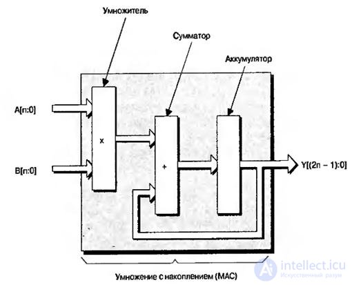
Fig.8.3. Functions that form the operation of multiplication with accumulation
When working with FPGA, which contains only embedded multipliers, to implement this function, it is necessary to connect the multiplier with an adder formed of several programmable logic blocks. The result will be stored in the triggers of logic blocks, or in blocks of embedded RAM.
An important feature of the FPGA is that in them almost all parts of the electronic device can be implemented in hardware (using logic gates, registers, etc.) or programmatically (in the form of microprocessor instructions). One of the main particular criteria for choosing between a hardware and software implementation of a function is the time it takes for this function to complete its tasks:
· Picosecond or nanosecond logic - must work extremely fast and is implemented in hardware in the structure.
· Microsecond logic is moderately fast and can be implemented both in hardware and software.
· Millisecond logic — used when implementing interfaces, such as polling switch states or igniting LEDs. The main efforts are aimed at slowing down the hardware when implementing these functions, for example, using huge counters to generate delays. Often, such tasks are best implemented on a microprocessor.
In fact, most devices in one form or another use microprocessors. Currently, FPGAs are available that contain one or more embedded microprocessors, commonly referred to as microprocessor cores. When using such FPGAs, it often makes sense to shift all tasks performed by an external microprocessor to the integrated microprocessor core. Such an approach provides a number of advantages, not least of which will be a reduction in cost, the elimination of a large number of tracks, seats and leads on a printed circuit board, as well as a reduction in the size and weight of a printed circuit board.
Distinguish between hardware and software implementation of microprocessor cores.
Hardware microprocessor cores are manufactured as separate predefined units. There are two ways to integrate such cores into FPGAs. The first one provides for the location of the core in the form of a strip (stripe) along one side of the main part, or the main structure of the FPGA (Fig.8.4). With this approach, all components are usually formed on the same silicon crystal. The main part of the FPGA also includes built-in RAM blocks, multipliers and other blocks.
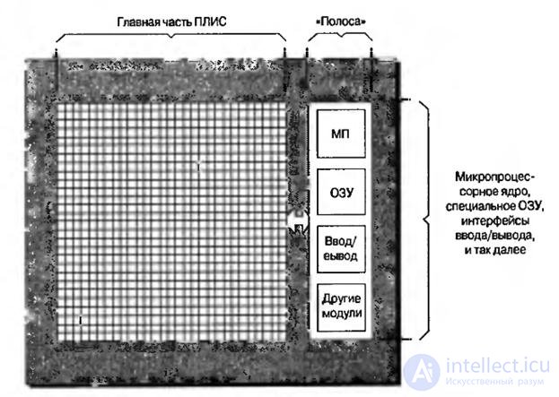
Fig.8.4. View of the crystal with a built-in core outside the main part
The advantage of this implementation is manifested in the main part of the FPGA, which turns out to be identical for devices with and without an integrated microprocessor core. This can significantly simplify the work of engineers with development tools. Another advantage is that FPGA vendors can bundle all additional functions, such as memory, I / O devices, and others, into one lane to supplement the microprocessor core.
The second method of integration is the embedding of one or more microprocessor cores directly into the main part of the FPGA (Fig. 8.5)
When using this method, the design tools used should take into account the presence of microprocessors in the structure of the chip. The memory used by the kernel is formed from built-in RAM blocks, and any pairing functions are implemented using groups of programmable general-purpose logic blocks. Proponents of this scheme argue that placing the microprocessor core in close proximity to the main part of the FPGA provides it with an advantage in speed.
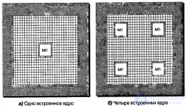
Fig.8.5. View of crystals with cores embedded in the main part
In addition to physically embedding a microprocessor into a chip structure, you can configure a group of programmable logic blocks to work as a microprocessor. This group is usually called the software kernel. Software kernels are simpler and slower than their hardware counterparts. However, they have one advantage - if necessary, you can implement a core or several cores in a volume that can be achieved until all resources are exhausted in the form of programmable logic blocks.
All synchronous elements inside the FPGA, for example, registers inside a programmable logic block, configured to operate as triggers, must be synchronized with a clock signal. Clock signals are usually generated outside of the chip and enter it through special synchronization inputs, and then distributed through special devices and fed to the corresponding registers.
Consider a simplified image of the synchronization tree (Fig. 8.6, programmable logic blocks are not shown).
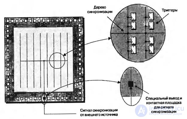
Fig.8.6. Simple sync tree
The name “synchronization tree” arose because the main clock signal forked like the branches of a tree, and the triggers can be considered as “leaves” at the ends of the branches. Such a structure instills confidence that all triggers will see their clock signals at the same time as possible. If the clock signals propagated through one long conductor, synchronizing all the triggers one by one, the trigger located closer to the chip synchronization output would see the clock pulse a bit earlier than the last triggers in this chain. This situation is called a phase shift, and it raises a number of problems. Even when using a synchronization tree, some phase shift may occur between registers located on the same branch, as well as between branches.
The synchronization tree is implemented using special conductors, which are separated from the general-purpose internal connections. The principle of operation, discussed above, is in fact greatly simplified. In practice, there are many synchronization pins in chips (unused synchronization pins can be used as general-purpose pins), and inside the device there are multiple synchronization domains (synchronization trees).
Chip clock output can be connected to the sync tree. However, as a rule, this pin is not connected directly to the synchronization tree, but to the input of the device (or block) of the synchronization control, called the synchronization manager, which generates child clock signals (Fig. 8.7).
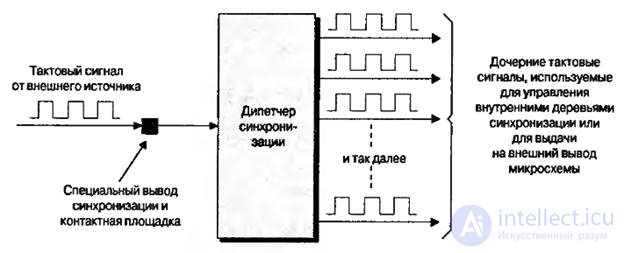
Fig.8.7. Synchronization manager generating child clocks
Child clocks can be used to control the internal trees (domains) of synchronization or to issue signals to external outputs of the chip, which, in turn, can be used to synchronize other devices located on the printed circuit board. Each FPGA chipset family has its own type of synchronization manager, and there can be multiple synchronization manager modules in one device. Different synchronization managers can support all or only some of the following devices that perform functions:
- elimination of fluctuations,
- frequency synthesis
- phase shift
- Phase shift auto-correction.
-
With the development of FPGAs based on static RAM cells in electronics, new opportunities have arisen related to dynamically reconfigurable logic. This refers to devices that can be reconfigured on the fly during system operation.
FPGA contains a large number of programmable logic elements and registers, which can be connected in different ways to implement various functions. It is noteworthy that components based on static RAM cells allow the system to load new configuration data into the device. Although all logic gates, registers and static memory cells that make up the FPGA are created on the surface of a single silicon crystal, it is sometimes useful to consider this device as consisting of two separate parts - logic gates (and registers) and programmable configuration cells of static RAM (Fig. 8.8).
Fig.8.8. Dynamically reconfigurable logic: FPGA based on static RAM cells
The flexibility of reconfigurable devices opens up truly wide possibilities. For example, at power up, the FPGA can be configured to test the system or self-test. As soon as the system completes testing, the FPGA can again be reconfigured to perform its basic functions.
Of course, the ability to reconfigure the functions of individual nodes on a printed circuit board provides additional amenities for engineers, but sometimes they need to create powerful systems that can be reconfigured at the circuit board level to perform different, radically different functions.
To solve this problem, it is necessary to configure the connections between devices at the circuit board level. So-called user-programmable interconnect devices (or field-programmable interconnect devices), which are also known as user-programmable interconnect chips (or field-programmable interconnect chips), can cope with this task. These chips, used to connect logical devices, can be dynamically reconfigured in the same way as standard FPGAs based on static RAM cells. Since each FPID chip can contain more than 1000 contacts, only a few such chips may be needed to connect components on a printed circuit board (Fig. 8.9).
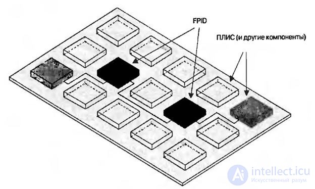
Fig.8.9. Dynamically reconfigurable connections: FPID based on static RAM cells
Interestingly, the described approach is not limited to the application at the level of printed circuit boards. Any of the above approaches can potentially be used in hybrid chips, and in multi-chip modules, and in single-chip devices.
One of the limiting factors for most FPGAs based on static RAM cells is the need to spend some time on reconfiguration. This feature is caused by the fact that the FPGA is usually programmed with the help of sequential data loading (or parallel data loading with a width of only 8 bits). When it comes to high-tech devices with tens of millions of static memory cell configurations, reprogramming can take several seconds. There are some types of FPGAs that solve this problem by using a large number of general-purpose I / O pins, which during programming form a wide configuration bus (say, 256 bits), and after configuration return to performing their basic functions.
Another disadvantage of the FPGA of the traditional architecture is that, if necessary, the most minor changes in the configuration have to be reprogrammed the entire device. Some FPGAs allow you to reconfigure them in columns, but in this case, a very rough level of structuring is provided. In addition, during the configuration, it is usually necessary to suspend the operation of the entire printed circuit board. Also, when programming, the contents of all FPGA registers are irretrievably lost.
To solve these problems, around 1994, Atmel Corporation (www.atmel.com) proposed a number of interesting FPGAs. In addition to supporting the dynamic reconfiguration of selected elements of internal logic, these devices are characterized by the fact that:
- does not disrupt the operation of the inputs and outputs of the device,
- system synchronization tools do not break,
- any parts of the device that are not subject to reconfiguration may continue their work,
- information of internal registers is not lost, even those that are in the reconfiguration area.
Of particular interest is the last item in this list, since it allows one function implementation to transfer data to another. For example, a group of registers can initially be programmed to operate as a binary counter. Then at some point in time determined by the main system, the same registers can be reconfigured to work as a linear shift register, the initial value of which is determined by the last contents of the counter before reconfiguration.
Although these devices became another evolutionary step in technological terms, in terms of their potential capabilities, the step turned out to be truly revolutionary.New terms such as virtual software and cache logic have been introduced to evaluate these capabilities.
Понятие “виртуальное программное обеспечение” возникло по аналогии с его программным эквивалентом – “виртуальной памятью”. Оба этих термина используются для представления предметов, которых на самом деле не существует. В случае виртуальной памяти компьютерная операционная система делает вид, что ей доступно больше оперативной памяти, чем есть на самом деле. Каждый раз, когда программа пытается получить доступ к ячейкам памяти, которых физически не существует, операционная система хитрит и меняет часть данных, находящихся в памяти, с данными, рамположенными на жёстком диске. Хотя эта процедура, известная, как ”свопинг”, замедляет процесс обработки данных, но в то же время позволяет программе выполнять свои задачи при меньшем объёме физичекой памяти.
Аналогично термин ”кэш-логика” произошёл от родственного ему понятия кэш-памяти, которая представляет собой высокоскоростную дорогостоящую статическую память для хранения текущих активных данных, в то время как основная часть данных помещается в более медленную недорогую память, например, в динамическую (DRAM).
Отслеживая местоположение и обращение к каждой микрофункции, а также объединяя функциональность и исключаяизбыточность, устройства с виртуальной аппаратной частью могут выполнять гораздо более сложные задачи, чем устройства, построенные по классической схеме. Например, в сложных функциях, требующих 100000 эквивалентных вентилей, в отдельный момент времени из них могут быть активными только 10000. Следовательно, с помощью сокращения или кэширования можно реализовать ещё функций на 90000 логических элементов. Тем самым небольшое и недорогое устройство с 10000 логическими элементами может заменить большое и дорогое со 100000 элементами (рис.8.10).
Таким образом возможно в реальном масштабе времени компилировать новые варианты устройств, которые могут быть использованы как динамически создаваемые аппаратные подпрограммы.
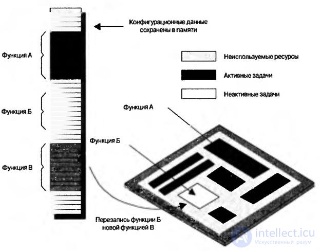
Рис.8.10. Виртуальное программное обеспечение
ПЛИС, классифицируемые как программируемые пользователем массивы узлов ( или FNPA – field-programmable node array), построены по крупномодульной архитектуре. Основополагающая концепция этих устройств состоит в том, что они сформированы из массива ”узлов”, каждый из которых является сложным элементом обработки данных (рис.8.11).
На рис.8.11 показано довольно упрощённое представление FPNA-устройства не только потому, что на нём не приведены элементы ввода/вывода и показано небольшое количество узлов обработки, хотя такое устройство может содержать сотни и тысячи подобных устройств. В зависимости от поставщика FPNA каждый узел может представлять собой арифметико-логическое устройство (АЛУ), микропроцессор или элемент алгоритмической обработки.
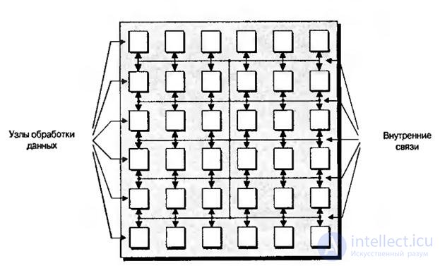
Рис.8.11. Общее представление устройства FPNA
Разработками в этом направлении занимается большое количество компаний. Далее будет рассмотрена продукция только двух копаний – PicoChip и QuickSilver, чьи концепции диаметрально противоположны.
Устройства picoArray компании picoChip формируются из массива процессоров и, в основном, предназначены для больших, не критичных к величине энергопотребления, стационарным системам, к которым относятся, например, базовые станции для беспроводных сетей. Кроме того, эти устройства при необходимости в любой момент могут быть реконфигурированы ( ежечасно или подобно тому).
В отличии от них ”адаптивные вычислительные машины” компании QuickSilver сформированы из кластеров узлов алгоритмических элементов. Применяются эти устройства в основном в небольших, неэнергоёмких портативных ихделиях, например, в фотоаппаратах и сотовых телефонах.Кроме того, эти устройства могут быть реконфигурированы сотни тысяч раз в секунду.
Устройства FPNA, главным образом, предназначены для реализации сложных алгоритмов, требующих значительных вычислительных ресурсов.
С одной стороны, существуют технологии, использующие алгоритмы пословной обработки, к числу которых, например, относится метод множественного доступа с разделением по времени ( или TDMA – time division multiple access), применяемый в системах беспроводной связи. С другой стороны, существуют технологии, использующие алгоритмы побитовой обработки, такие как метод широкополосного множественного доступа с кодовым разделением каналов ( или W-CDMA – Wideband Code Division Multiple Access) и его подвиды CDMA2000, IS-95A и другие. Существуют также технологии, использующие алгоритмы, представляющие смесь пословной и побитовой обработки данных, например, различные виды MPEG, сжатие речи, музыки и так далее.
That is, complex algorithms can be substantially heterogeneous (heterogeneous) in nature. Based on this, it is obvious that heterogeneous structures must also be used to implement heterogeneous technologies.
Для удовлетворения требований к обработке описанных выше алгоритмов, компания picoChip использует устройство под названием picoArray. Его гетерогенная узловая архитектура представляет собой матрицу различных 16-битных RISC (Reduced Instruction Set Computing – технология вычислений с сокращённым набором команд) микроконтроллеров, каждый тип которых оптимизирован для реализации определённых вычислений. Например, один из них может содержать много памяти, а другой будет поддерживать специальные алгоритмические команды типа ”расширение” и “сужение” для беспроводного стандарта CDMA, используя для этого один такт ( в отличии от 40 тактов при использовании универсального процессора).
Операторы сотовой связи тратят миллиарды долларовежгодно на развитие своих беспроводных инфраструктур, причём, большая часть этих сумм уходит на разработку новых модулей цифровой обработки, устанавливаемых на базовых станциях. В зависимости от расположения каждая базовая станция должна предусматривать обработку десятков или сотен каналов одновременно.
Поэтому неудивительно, что у всех заинтересованных лиц есть огромное желание уменьшить стоимость реализации каждого канала. Так как один picoArray может заменить несколько традиционных заказных микросхем, ПЛИС и процессоров ЦОС, его использование как раз и позволяет существенно снизить цену канала базовой станции.
При обычном подходе заказные микросхемы позволяют достичь очень высокой производительности, но они отличаются высокой стоимостью и длительными сроками разработки. К тому же алгоритмы, реализованные в заказных микросхемах, жёстко прошиваются в схему. Это, пожалуй, самая главная проблема заказных микросхем, так как стандарты беспроводной связи меняются настолько быстро, что к моменту завершения разработки заказной микросхемы она уже может устареть.
В отличие от заказных микросхем у picoArray каждый микропроцессорный узел может быть легко реконфигурирован для адаптации к ежечасным изменениям пользовательских профилей, к еженедельным расширениям и исправлениям ошибок, и к ежемесячным этапам развития беспроводных протоколов. Следовательно, базовые станции, построенные по технологии picoArray, имеют более долгий срок эксплуатации, что позволяет снизить затраты на работу системы связи.
Архитектура адаптивной вычислительной машины (АВМ) в обощённом виде представлена на рис.8.12. На самом нижнем уровне находится узел алгоритмических элементов. Четыре таких узла, составляющих квадрант, соединённый матрицей внутренних соединений, формируют структуру, которую можно назвать кластером первого уровня. Четыре таких кластера первого уровня могут быть сгруппированы в кластер второго уровня и так далее.
Каждый из алгоритмических узлов выполняет задачи на уровне целых алгоритмических элементов, типа фильтров с конечной импульсной характеристикой, дискретного косинусного преобразования и т.д. Кроме того, узел может применяться для реализации нелинейных арифметических функций, таких как (1/sinA)·(1/x) и полученное произведение возвести в 13-ю степень.
Аналогично узел обработки битов может применяться для реализации различных функций побитной обработки, например, линейного сдвигового регистра, кодового генератора Уолша, дешифратора TCP/IP –пакетов и т.п.
Каждый узел окружён оболочкой, которая позволяет со стороны внешнего мира рассматривать все узлы совершенно одинаковыми. Эта оболочка принимает входящие пакеты информации ( команды, необработанные данные, конфигурационные данные и т.д.) из внешнего мира, распаковывает их, рапределяет по узлу, управляет задачами обработки, собирает результаты и возвращает их во внешний мир.
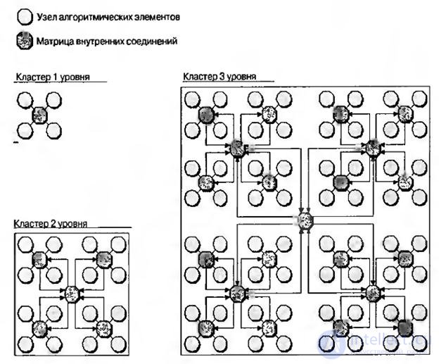
Рис.8.12. Архитектура адаптивной вычислительной машины.
Один из ключевых моментов технологии АВМ заключается в том, что любая часть устройства, от нескольких узлов до целой микросхемы, может быть быстро адаптирована для решения определённой задачи в большинстве случаев за один такт. Также любопытно, что 75% каждого узла реализуется в локальной памяти. Эти особенности позволяют вносить радикальные изменения в методы реализации алгоритмов. В отличие от обычного способа передачи данных от функции к функции, при таком подходе данные могут оставаться в узле, в то время как функция узла может меняться с каждым тактом. Это также значит, что в отличии от заказных микросхем, в которых для каждого алгоритма требуется отдельный кристалл, возможность адаптировать АВМ десятки или сотни тысяч раз в секунду подразумевает, что только те части алгоритма, которые действительно выполняются, должны оставаться в устройстве в текущий момент времени. Этот подход позволяет существенно снизить величину потребляемой мощности и занимаемое на кристалле место.
В дополнение к структуре, изображенной на рис.6.37, любая адаптивная вычислительная машина включает в себя группу узлов специального назначения, таких как системный конроллер, контроллер внешней и внутренней памяти, а также узлы ввода/вывода. Каждый узел ввода/вывода может использоваться для реализации задач ввода/вывода данных в форме универсального асинхронного приёмопередатчика (УАПП) или в виде шинного интерфейса, например, PCI, USB, Firewire и им подобных (как и алгоритмические узлы, узлы ввода/вывода при необходимости могут быть реконфигурированы в течении одного такта). Кроме того, эти узлы используются для импорта конфигурационных данных, так как у каждой АВМ ширина шины конфигурации может быть равна количеству входных контактов.
Каждая АВМ содержит встроенную операционную систему (ОС), которая распределена по узлу системного контроллера и оболочкам, связанных с каждым алгоритмическим узлом. Алгоритмические узлы также планируют свои задачи и все межузловые соединения. Это позволяет разгрузить работу узла системного контроллера, основная обязанность которого заключается в отслеживании свободных в текущий момент узлов и распределение между ними новых заданий.
Из рис.8.12 следует, что ядро архитектуры АВМ может легко масштабироваться. При этом желательно, чтобы установленные на печатной плате микросхемы различных АВМ взаимодействовали между собой и с остальной частью схемы на уровне операционных систем. В этом случае их работу можно рассматривать как работу отдельных устройств.
1. Describe the options for embedding RAM blocks, multipliers, adders and microprocessor cores into the FPGA.
2. Synchronization features in FPGA.
3. The concept of a user-programmable array of nodes.
4. The architecture of the adaptive computing machine.

Comments
To leave a comment
Computer circuitry and computer architecture
Terms: Computer circuitry and computer architecture