Lecture
Under combinational understand nodes that do not contain memory elements. In such nodes, any change in the state of the input signals causes a corresponding change in the output signals with a delay determined by the duration of the transient processes in the given node. In the general case, a combinational node (CU) contains several inputs and several outputs. The behavior of a combinational knot is described by functions of the algebra of logic (Boolean or logical functions). In this case, for each output it is possible to determine the corresponding Boolean function, which completely determines the behavior of the combinational node on this output without taking into account the signal propagation delay, that is, for an ideal node.
The delay time of the signal for each output may be different. The delay time depends on which input signal, by changing its state, led to a corresponding change in this output signal.
The behavior of the combinational node can be defined by a truth table, in which each combination of values of input signals is assigned the value of each output variable. Input variables will be denoted by the letter X with the corresponding index, and output variables by the letter Y with the corresponding index. According to the well-known truth table, it is possible to compose a corresponding boolean function for each output. The number of combinational nodes that can be synthesized is huge, even with a fairly small number of input variables. But practice in most cases does not require the actual development of a new combinational node, and it suffices to restrict ourselves to the use of well-known circuit solutions implemented in the form of microcircuits. It is enough to use standard chips wisely.
Select the following combinational nodes, which are implemented in the form
microcircuits: decoders and encoders, multiplexers and demultiplexers, bus drivers, digital signal comparators, adders, arithmetic logic units and multipliers.
Information, address and control inputs can be distinguished in the combinational nodes. Control inputs are labeled E (Enable). Information and address inputs are labeled with numeric labels, which can indicate the number in order or weight of the binary variable supplied to this input. The weight is indicated either by the power of two, into which the two should be built to obtain the real weight of the discharge, or by the actual value of the weight of the discharge. For the inputs and outputs of the node, you can define the concept of active and passive signal. Under the active understand the level of the signal, which causes certain actions or interest. If the unit level is active, then the corresponding output is direct and is depicted as the direct input of the work permit is shown in Figure 3.1, a. If the zero level is active, then the corresponding output is marked with an inverting circle, as shown in Figure 3.1, b. Direct inverse input input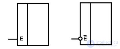 a) b) Fig. 3.1.-Examples of image resolution inputs
Encoders (coders) are devices designed to convert alphanumeric information filed by a unitary n-bit code to an equivalent binary m-bit code. A feature of the unitary code is the active state of only one variable X i of the input set {X n -1 ... X 1 X 0 } , the sequence number of which is to be encoded. Those. The encoder nm is a converter of the unitary code “1 from n” to binary (parallel) code, in which the number of outputs m is uniquely related to the number of inputs n as 2 m . For n = 2 m , the full set of output binary combinations Y i is used . Such an encoder is called complete . For example, the 8-3 encoder is full, because it implements the full set of possible combinations of variables X i (n = 8) into the full output set Y i (m = 3) as 2 3 = 8 .
In the incomplete encoder, the number of inputs n does not correspond to the number of all possible output combinations 2 m (n <2 m ) , which accordingly creates a certain number of unused output sets. An example of an incomplete encoder is the encoder 10-4 , used to encode decimal numbers into binary code (8-4-2-1) .
In the synthesis of a complete (incomplete) encoder, it is sufficient to implement in a given basis a system of logical functions Y i , which create the word {Y m -1 ... Y 1 Y 0 } on its m outputs. For example, the full 8-3 encoder is described by a truth table (Table 3.1) and a system of logical functions:

 ;
;
 ; (3.1)
 .
.
Table 3.1 The Truth Table of the Complete Encoder 8-3
| Number | Inputs | Outputs | |||||||||
| X 0 | X 1 | X 2 | X 3 | X 4 | X 5 | X 6 | X 7 | Y 2 | Y 1 | Y 0 | |
From the system of logical functions, it follows that the encoder 8-3 is implemented in the basis of LE 4ILI (Fig. 3.1). Y 0 - the output of the lower order weighing 2 0 , Y 1 - 2 1 and Y 2 - the output of the senior discharge weighing 2 2 .
The incomplete coder is implemented in the same way as the full coder, however, those sets of variables that are not used in coding are missing. In the encoder 10-4, the unused output sets will be 2 4 -10 = 6 - Y i : {1010}, {1011}, {1100}, {1101}, {1110}, {1111} .
Given in fig. 3.1 encoder - linear , all LEs are connected to one common bus (lines). To implement a linear encoder, you must have multi-input LEs. The variable X 0 is not involved (Table 3.1). This means that for any signal at input X 0, there will be no changes at the output of the encoder.
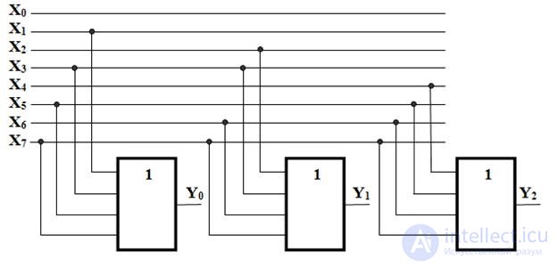
Fig. 3.1. Functional scheme of the full encoder
The pyramidal encoders , built on the principle of using the same type, for example, two-input LE 2I-NOT, have lower coding speed. The structural scheme of such encoders is similar to a pyramid. The number of LEs does not depend on the digit capacity of the m coded word.
In linear and pyramidal encoders, the output m-bit code must be matched to a single active input. In order for the encoder to react only to one of several active inputs, its scheme is built according to the priority principle.
In the priority encoder, the output code always corresponds to the active input that has the largest dialing number. For example, at the output of the priority encoder with the inputs X 1 , X 2 , X 4 active , the code {100} will appear, which corresponds to the variable X 4 (the active inputs X 1 and X 2 are ignored).
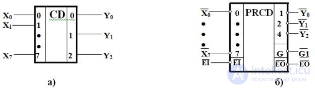
Fig.3.2. Conditional graphic image of the full (a) and priority (b) encoders
In the industrial series of elements there are priority encoders for eight-bit and ten-bit words. The operation of the eight-bit priority encoder is described by a truth table (Table 3.2).
Table 3.2 The truth table of the eight-bit priority
encoder
| EI | X 7 | X 6 | X 5 | X 4 | X 3 | X 2 | X 1 | X 0 | Y 2 | Y 1 | Y 0 | G | Eo |
| X | Xx | XXX | Xxxx | XXXXX | XXXXXX | XXXXXXX | XXXXXXXX |
Table 3.2 describes the operation of the priority encoder for all possible combinations of signals. Figure 3.2, b shows its conventional graphic image, the signal EI - the resolution of the encoder; HU - the signal generated at the output of the encoder in the absence of requests for its inputs serves to enable the next (minor) encoder to work when increasing the size of the encoders; G - signal indicating the presence of requests at the entrance; X 0 ... X 7 - requests for inputs; Y 2 ... Y 0 - values of the bits of the output binary code generated by the number of the highest active request. All of these signals are formed under the condition EI = 1 (work is allowed). When EI = 0, regardless of the state of the request inputs, all output signals become zero.
From table 3.2, you can write expressions for Y 2 , Y 1 , Y 0 , EO and G :


 (3.2)
(3.2)
 ;
;
 +
+  +
+  +
+  +
+  +
+  +
+  +
+  .
.
Linear encoders are used to transfer information in the interface devices, when compressing information transmitted via a small number of communication lines.
Priority encoders can be used for digital-analog and analog-digital conversion, as well as for the implementation of priority coding and interruption in microprocessor circuitry.
Decoders (decoders) - devices for recognizing the number filed by the positional n- digit code. Decoders are code converters. The decoder nm performs the function of converting a binary code into a unitary code “1 of m” , i.e. performs the opposite function of the encoder. For a complete decoder, m = 2 n , where m is the sequence number of the output Y i of the decoder. In an incomplete decoder, the number of outputs m does not correspond to 2 n (m <2 n ) .
In the conventional graphic notation (Fig. 3.3, b), the inputs of the decoder are designated by binary weights. In addition to the information inputs, the decoder usually has one or more work enable inputs ( EN ). If there is permission for this input, the decoder works in the manner described above, in its absence, all outputs of the decoder are passive. If there are several permit inputs, then the work enable signal is formed as a combination of signals from separate enable inputs. Often the decoder has inverse outputs. In this case, only one output has a zero value, and all the others have a single value, and if it is disabled, all the outputs will have a logical one. The operation of the complete decoder (n - m) is described by system (3.3):
 ;
;
 ;
;
 ;
;
…………………………………………………………;
 .
.
As follows from the conjunction system (3.3), each of the m outputs of the full decoder corresponds to one of 2 n code combinations (minterm or maxsterm) n - bit input word {X n -1 ... X 1 X 0 } .
An incomplete decoder has a number of unused input sets.
Diagrams of complete or incomplete decoders as well as encoders can be assembled along a linear or pyramidal structure.
The number of outputs of the full four-digit decoder is 16 (2 4 = 16). The complete decoder 4-16 is described by the system of Boolean functions (3.4):


Figure 3.3, a shows a functional diagram of a complete decoder 4-16, operating in accordance with table 3.3.
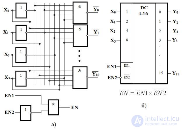
Fig. 3.3. Functional diagram of the complete decoder 4-16 (a), conditional graphic designation of the binary decoder 4-16 (b)
Table 3.3 Truth table of the complete decoder 4-16
| X 3 | X 2 | X 1 | X 0 | Y i |
 |
||||
 |
||||
 |
||||
 |
||||
 |
||||
 |
||||
 |
||||
 |
||||
 |
||||
 |
||||
 |
||||
 |
||||
 |
||||
 |
||||
 |
||||
|
|
In cases when it is necessary to create a decoder for a larger number of outputs based on decoders with a smaller number of outputs, the principle of extension is used . It lies in the fact that these inputs of the decoders are divided arbitrarily into groups, each of which implements its own group of logical functions.
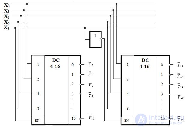
Fig. 3.4. Functional two-stage decoder circuit
Figure 3.4 shows the two-stage connection of two decoders. The first stage operates with active inputs X 0 , X 1 , X 2 and X 3 , provided that X 4 = 0. As soon as the code appears on the inputs of the decoder  , the first cascade will close, because
  , the second stage will open, which will receive a permit level through the inverter
  .
.
Decoders are used in visual display devices, together with the OR circuits they can be used to reproduce arbitrary logical functions.
Linear decoders provide code conversion with minimal latency and are used in the fastest digital circuits. However, with an increase in the input code capacity, the load of each of the inputs and the number of integrated circuit packages (IC) for the implementation of the decoder rapidly increase. Linear structure is usually used to build decoders with the number of inputs ≤4 .
If the number of inputs > 4 , then in order to reduce the number of IC cases, the decoders are performed according to a multi-stage scheme. Such decoders are called pyramidal . The first step of the pyramidal decoder is the simplest linear decoder. Each subsequent stage, controlled by an additional input variable, allows you to double the number of outputs, i.e. The k- step full pyramidal decoder has the number of outputs N = 2 k +1 , moreover, k = m-1 (for m = 2, the linear and pyramidal decoders are the same).
Code converters are used to convert binary codes into binary additional, binary-decimal, codes of characters of the Russian or Latin alphabet, number codes of any number system and vice versa.
The principle of constructing code converters will be considered on the example of the conversion of the code 8421 to the code 2421 . Denote the variables corresponding to the individual digits of the code 8421 , - X 4 X 3 X 2 X 1 , and the code 2421 - Y 4 Y 3 Y 2 Y 1 . The truth table (Table 3.4) shows the correspondence of combinations of both codes.
Table 3.4 The truth table of the converter code 8421 to code 2421
| Code 8-4-2-1 | Code 2-4-2-1 |
| X 4 X 3 X 2 X 1 | Y 4 Y 3 Y 2 Y 1 |
| 0 0 0 0 0 0 0 1 1 0 1 1 1 0 0 0 1 1 0 1 1 1 1 1 0 0 1 1 0 1 | 0 0 0 0 0 0 0 1 1 1 1 1 1 1 1 1 1 1 1 1 1 |
Each of the variables Y 4 , Y 3 , Y 2 , Y 1 can be considered a function of the arguments X 4 , X 3 , X 2 , X 1 and, therefore, is represented through these arguments by a corresponding logical expression. To obtain the specified logical expressions, we present the variables Y 4 , Y 3 , Y 2 , Y 1 by truth tables in the form of a Carnot map (Fig. 3.5) 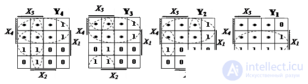
Fig. 3.5. Carnot cards for code converter 8-4-2-1 to code 2-4-2-1
Using Carnot maps, we obtain the minimum form of logical expressions in the basis of AND, OR, NOT (3.5) and, having performed the transformation 3.5, using the de Morgan rule, we obtain the same expressions in the basis of NAND (3.6).
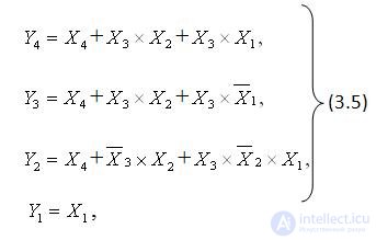
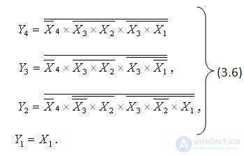
Figure 3.6 shows the logical structure of the code converter built on the NAND elements using the obtained logical expressions.
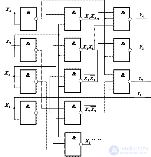
Fig. 3.6. The logical structure of the code converter 8-4-2-1 to code 2-4-2-1 in the basis of the elements AND IS NOT
Дешифраторы со схемами ИЛИ можно использовать для воспроизведения произвольных логических функций. Действительно, на выходах дешифратора вырабатываются все конъюнктивные термы, которые только можно составить из данного набора аргументов. Логическая функция в совершенной дизьюнктивной нормальной форме (СДНФ) есть дизъюнкция некоторого числа таких термов. Собирая термы по схеме ИЛИ, можно получить любую функцию данного числа аргументов.
In fig. 3.7 в качестве примера показана схема выработки двух функций  and
and  . Такое решение может быть целесообразным при необходимости выработки нескольких функций одних и тех же аргументов. В этом случае для выработки дополнительной функции добавляется только один дизъюнктор. Заметим, что для проверки правильности схемы рис. 3.7 удобно перевести функции F 1 и F 2 в СДНФ.
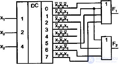
Fig.3.7 Diagram of the generation of functions F 1 and F 2 using a decoder and OR schemes
Мультиплексор (коммутатор) – универсальное логическое устройство, на основе которого создают различные комбинационные и последовательные схемы, имеют один выход ( Y 1 ) и более одного входа и осуществляющее коммутацию под действием управляющих сигналов ( Х k -1 , Х k -2 , …, Х 1 , Х 0 ) одного из информационных входных сигналов ( D 0 , D 1, …, D 2 k -1 ) - на выход. Обычно 2 k =n , где k и n – число управляющих и информационных входов соответственно. Код, поступающий на управляющие входы, определяет один из информационных входов, значение переменной которого передаётся на выход Y 1 .
C помощью мультиплексоров осуществляется разделение во времени информации, поступающей по разным каналам. Часто используются для преобразования параллельного кода в последовательный, в делителях частоты, триггерных и сдвигающих устройствах и пр.
Набор сигналов, поступающих на управляющие входы, задаёт двоичное число вида:
 , (3.7)
где Х i * =(0,1)- значение сигнала на входе Х і . Выходной сигнал мультиплексора повторяет сигнал информационного входа D с номером Х * .
Функция, реализуемая мультиплексором, может быть представлена в виде
 +
+  +…+
+…+
+  =
=  +
+  +
+  + … +
+ … +  , (3.8)
где R j –конъюнкция, равная 1 на наборе значений переменных Х k -1,
Х k -2, …,Х 0 c номером j (т.е. на наборе, представляющем в двоичном виде число j ).
Таблица истинности, описывающая работу мультиплексора, имеющего n=8 информационных и k=3 управляющих входов имеет вид, представленный в табл. 3.5. Часто мультиплексоры строятся с использованием элемента типа И-ИЛИ для коммутации сигналов и дешифратора для управления коммутацией. In fig.3.8 is a functional multiplexer circuit with two control inputs X 0 , X 1 and its conventional graphic designation.
Table 3.5 The truth table of a multiplexer with n = 8 information and k = 3 control inputs
| X 2 | X 1 | X 0 | D 0 | D 1 | D 2 | D 3 | D 4 | D 5 | D 6 | D 7 | Y 1 | |
| x | x | x | x | x | x | x | ||||||
| x | x | x | x | x | x | x | ||||||
| x | x | x | x | x | x | x | ||||||
| x | x | x | x | x | x | x | ||||||
| x | x | x | x | x | x | x | ||||||
| x | x | x | x | x | x | x | ||||||
| x | x | x | x | x | x | x | ||||||
| x | x | x | x | x | x | x | ||||||
| x | x | x | x | x | x | x | ||||||
| x | x | x | x | x | x | x | ||||||
| x | x | x | x | x | x | x | ||||||
| x | x | x | x | x | x | x | ||||||
| x | x | x | x | x | x | x | ||||||
| x | x | x | x | x | x | x | ||||||
| x | x | x | x | x | x | x | ||||||
| x | x | x | x | x | x | x | ||||||
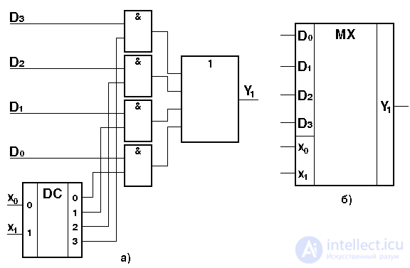
Fig. 3.8. Functional four-channel multiplexer circuit with two control inputs (a) and its conventional graphic designation (b)
If it is necessary to expand the number of inputs, then cascade switching on of multiplexers is used. Figure 3.9 shows a four-input multiplexer circuit based on two-input multiplexers.
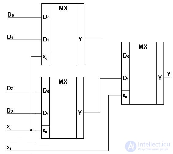
Fig.3.9. Multiplexer cascade connection scheme
Демультиплексор – комбинационная схема, выполняющая функцию, обратную функции мультиплексора, т.е. это комбинационная схема, имеющая один информационный вход ( D 1 ), n информационных выходов ( Y 0 , Y 1 , Y n -1 ), и k управляющих входов ( X k -1 , X k -2 , … X 1 , X 0 ). Обычно, также как и у мультиплексоров, 2 k =n . В зависимости от кода k на управляющих входах сигнал с единственного информационного входа выдаётся на один из n выходов.
Demultiplexers are often used to convert serial code to parallel.
The combination scheme of the demultiplexer implements the function (3.9):
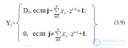
The work of the demultiplexer is described by the logical equations (3.10): 


……………………………


The truth table describing the operation of the demultiplexer with n = 8, k = 3 , is represented by table 3.6.
Table 3.6 The truth table of the demultiplexer with n = 8, k = 3
| D 1 | X 2 | X 1 | X 0 | Y 0 | Y 1 | Y 2 | Y 3 | Y 4 | Y 5 | Y 6 | Y 7 |
As demultiplexers can be used decoders - demultiplexers.
На рисунке 3.10 представлена схема функциональная демультиплексора с четырьмя информационными выходами и двумя управляющими входами и его условное графическое изображение.
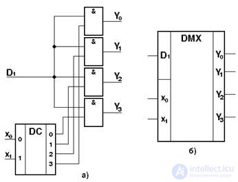
Fig. 3.10. Схема функциональная демультиплексора с прямыми управляющими входами (а) и его условное графическое изображение (б)
Для наращивания числа выходов демультиплексора используют каскадное включение демультиплексоров. На рисунке 3.11 приведена схема демультиплексора с шестнадцатью выходами на основе демультиплексоров с четырьмя выходами.
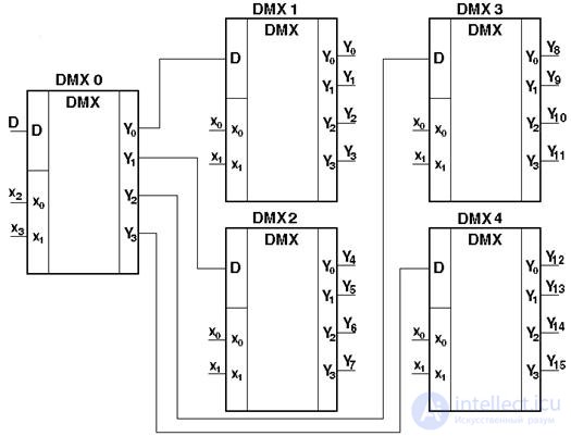
Fig. 3.11. Схема каскадного включения демультиплексоров
Функции демультиплексоров сходны с функциями дешифраторов. Дешифратор может рассматриваться как демультиплексор, у которого информационный вход поддерживает напряжение выходов в активном состоянии, а адресные входы выполняют роль входов дешифратора.
Мультиплексоры предназначены для объединения нескольких выходов в тех случаях, когда заранее известно количество выходов, которые нужно объединять. Часто это неизвестно. Более того, часто количество объединяемых микросхем изменяется в процессе эксплуатации устройств. Наиболее яркий пример - это компьютеры, в которых в процессе эксплуатации изменяется объем оперативной памяти, количество портов ввода-вывода, количество дисководов. В таких случаях невозможно для объединения нескольких выходов воспользоваться логическим элементом "ИЛИ". Одним из вариантов решения этой проблемы является использование микросхем, имеющих выходы с открытым коллектором. Недостатком такого объединения нескольких микросхем на один провод является низкая скорость передачи информации, обусловленная затягиванием переднего фронта.
Эта проблема исчезает, если для объединения выходов применить элементы, имеющими выходы с тремя состояниями. Такие элементы называются шинными формирователями.
Основное назначение шинных формирователей – увеличение нагрузочной способности шин в микропроцессорных и других цифровых устройствах, отключение источников и приемников информации от шин за счет наличия третьего состояния, обеспечение двунаправленного обмена информацией.
In fig. 3.12,б представлена функциональная схема шинного формирователя (ШФ) на микросхеме К589АП16, представляющая собой четырехбитную двунаправленную схему, каждая линия которой содержит две логические схемы И с мощным выходом и тремя логическими состояниями. С одной стороны входы и выходы схем И объединены ( DB1…DB4 ) и используются для интерфейса формирователя со схемами, совместимыми с ТТЛ. С другой стороны входы DI1…DI4 и выходы DO1…DO4 разделены для максимальной гибкости использования кристалла.
Назначение входов и выходов кристалла следующие: DI1…DI4 – информационныевходы, DO1…DO4 – информационные выходы, DB1…DB4 – информационные входы-выходы реверсивной передачи информации; CS – выбор кристалла; BS – вход управления передачей информации. Если внимательно посмотреть на представленную функциональную схему шинного формирователя, то нетрудно рассмотреть, что данная схема представляет собой мультиплексор с двумя входами: DI и DB , выходом DO и управляющим сигналом BS . Режимы работы ШФ К589АП16 сведены в таблице 3.7.
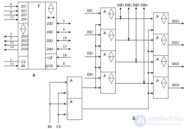
Fig. 3.12. Условное обозначение (а) и функциональная схема (б) шинного формирователя К589АП16
Таблица 3.7 Режимы работы ШФ К589АП16
| Логическое состояние по входам логики управления | Направление передачи информации | |
| CS | BS | |
| Передача от входов DI на выходы DB | ||
| Передача от входов DB на выходы DO | ||
| X | Отсутствие передачи (высокоинпедансное состояние) |
Кроме коммутационных функций, мультиплексоры позволяют реализовать комбинационные устройства на m (m – количество управляющих входов) входов и на один выход. Если комбинационное устройство, построенное на базе мультиплексора, не требует подключения дополнительных элементов логики, то оно называется универсальным логическим модулем (УЛМ). Отметим, что мультиплексор 8®1 (3 управляющих и 8 информационных входов) позволяет реализовать любую функцию трёх переменных.
Для получения УЛМ управляющие входы мультиплексора представляют как информационные, а информационные входы - как настроечные (следовательно, у мультиплексора 8 ®1 будут три информационных и 8- настроечных входов).
Пусть функция задана в виде карты Карно (рис. 3.13).
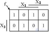
Fig. 3.13. Карта Карно функции, реализуемой мультиплексором
При построении УЛМ на карте Карно минимизационные контуры не проводятся. По карте записывается СHДФ с учетом состояния информационных (настроечных) входов мультиплексора.

Сопоставляя полученную СHДФ с формулой мультиплексора (3.8), определяем номера коэффициентов “а”, т.е. D 0 =a 1 , D 3 =a 2 , D 5 =a 3 , D 6 =a 4 . Следовательно, эти коэффициенты равны единице, т.е. D 0 = D 3 = D 5 = D 6 = 1, а на остальных настроечных входах логические нули, т.е. D 1 = D 2 = D 4 = D 7 = 0.
Схема комбинационного устройства, построенного на базе мультиплексора 8-1 и реализующего функцию f , приведена на рис. 3.14.
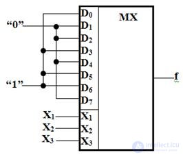
Fig. 3.14. Схема соединения настроечных входов мультиплексора, реализующую функцию f
Как следует из рис. 3.14, построение комбинационного устройства на базе мультиплексора сводится к объединению настроечных входов так, чтобы получилось две группы. К одной группе входов, в соответствии с заданной функцией, подают логический “0”, а другой - “1”.
На базе мультиплексоров можно синтезировать комбинационные устройства, которые могут реализовать функции на большее число переменных, чем количество управляющих входов мультиплексора. Очевидно, и в этом случае, мультиплексор сохраняет свою универсальность, так как часть переменных реализуемой функции непосредственно подается на входы Х 1 . . . Х m мультиплексора (количество переменных, непосредственно подаваемых на управляющие входы мультиплексора равно m ).
Часто использование мультиплексора при синтезе КУ, реализующего функцию с числом переменных больше, чем число управляющих входов мультиплексора, существенно упрощает этот процесс и схему.
В общем случае, когда требуется синтезировать КС, реализующее функцию N аргументов на мультиплексоре с M управляющими входами и 2 М информационными входами, М младших переменных из набора Х 1 , Х 2, ... Х N следует подать на управляющие входы, а информационные сигналы (настроечные) D 0 , D 1 , . . . . D 2 м нужно представить функциями остальных ( N - M ) переменных, как показано на рис. 3.15. Тогда синтез КС сводится, по сути дела, к синтезу схемы формирования информационных сигналов, которую можно рассматривать как внутреннюю более простую КС.
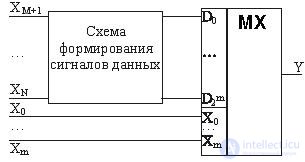
Fig. 3.15. Общая схема комбинационного устройства на мультиплексоре, реализующего функцию N переменных
продолжение следует...
Часть 1 Theme 3. Circuit design combinational nodes
Часть 2 3.7. Компараторы - Theme 3. Circuit design combinational nodes
Часть 3 3.11.2.5 Быстродействие - Theme 3. Circuit design combinational nodes


Comments