Lecture
LAD commands consist of elements and blocks that are graphically combined into segments. Elements and blocks can be divided into the following groups:
Commands as elements - these commands of the contact plan are presented as separate elements that do not need addresses or parameters.
| Element |
 |
Commands as elements with an address - these commands of the contact plan are presented as separate elements for which you need to enter an address.
| Element |
 |
Commands as elements with address and value - these commands of the contact plan are presented as separate elements for which you need to enter the address and value
| Element |
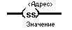 |
Commands in the form of blocks with parameters - these commands in the form of blocks with lines of inputs and outputs. The inputs are on the left side of the unit; outputs on the right side of the unit. You fill in the input parameters. For the output parameters, you specify the places where the STEP 7 software can put the output information for you. For these parameters, you must use a notation that corresponds to individual data types.
| Element |
|
Commands in the form of blocks with parameters
STEP 7 presents some commands of the contact plan in the form of blocks with lines of inputs and outputs (see Table 2-4). The inputs are on the left side of the unit; outputs on the right side of the unit. You fill in the input parameters. For the output parameters, you specify the places where the STEP 7 software can put the output information for you. For these parameters, you must use a notation that corresponds to individual data types. How the EN (allow input) and ENO (allow exit) parameters work is explained below. 
Allow Sign In and Allow Sign Out options
The transfer of energy to the enable input (EN) of the block of the contact plan (activation) leads to the fact that the block performs the specified function. If the unit is able to perform its function without errors, then the enabling output (ENO) transmits energy through the circuit. The block parameters КОР EN and ENO are of type BOOL and can be located in the memory area I, Q, M, D or L
EN and ENO operate in accordance with the following principles:
Restrictions for blocks and coils
You cannot place blocks and connectors in a circuit in a circuit that does not start on the left supply line. An exception is the comparison operation.
Memory areas and their functions
Most of the addresses in the LAD relate to memory areas. The following table shows their types and functions.
The LAD program monitors how the flow of energy passes between the supply bus through various inputs, outputs and other elements and blocks. Many commands of the contact plan operate in accordance with the principles of Boolean logic.
Each logical operation polls the signal state of the electrical contact to 0 (not activated, turned off) or 1 (activated, turned on) and then gives the result. Then the operation either saves the result or uses it to perform a boolean logical operation. The principles of Boolean logic are demonstrated here using make and break contacts.
Normally open (make) contact
The figure shows a relay-contact circuit with one relay contact between the supply bus and the coil. In normal condition, this contact is open. If the contact is not activated, it remains open. The signal state of the open contact is 0 (not activated). If the contact remains open, the energy from the supply bus cannot energize the coil at the end of the circuit. If the contact is activated (the state of the contact signal is 1), then the current will flow through the coil. The figure shows a normally open contact relay, as it is sometimes represented on the relay-contact diagrams.
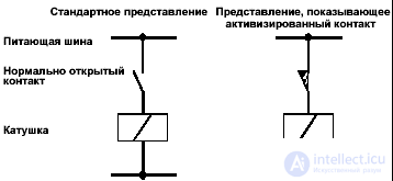
You can use the Normally Open Contact command to poll the signal state of a normally open contact of the control relay. Interrogating the state of the signal, the team determines whether the current can flow through the contact or not. If current can flow, the command gives the result 1; if the current cannot flow, the command gives the result 0. The command can save this result or use it to perform a boolean logic operation.
This element is the inverse of the open contact. That is, if if the signal is 0, then the result of the operation is 1.
| Team | The result if the signal state contact is 1 (contact activated) | The result if the signal state contact is 0 |
| - | | | - | 1 (The available energy can be transferred because the normally open contact is closed). | 0 (The available energy cannot be transferred because the normally open contact is open.) |
| - | / | - | 0 (The available energy cannot be transferred because the normally closed contact is open). | 1 (The available energy can be transferred because the normally closed contact is closed.) |
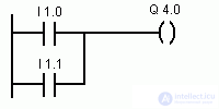
With normally open contacts, you can create a logical AND operation or a logical OR operation.
In order to create a logical operation And connect successively two normally open contacts, as shown in the figure.
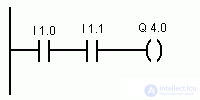 | The logical operation is shown here. And the result is 0. | |
 | Contacts that are activated are highlighted in a different color. | |
| If both contacts are activated, then at output Q 4.0 the result will be equal to 1, that is, a current can flow through this circuit. | ||
| Truth table for and | ||
| Contact I 1.0 | Contact I 1.0 | Coil Q 4.0 |
| 0 | 0 | 0 |
| one | 0 | 0 |
| 0 | one | 0 |
| one | one | 0 |
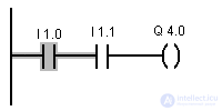
Logical operation OR can be obtained by connecting the contacts in parallel.
 | If at least one of the I 1.0 or I 1.1 contacts has a signal, then at the output of Q 4.0 the RLO signal is 1. |
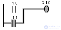 | the current path is highlighted in a different color. |
| Truth table for OR | ||
| Contact I 1.0 | Contact I 1.0 | Coil Q 4.0 |
| 0 | 0 | 0 |
| one | 0 | one |
| 0 | one | one |
| one | one | one |
Registers help the CPU perform logical and arithmetic operations, shift operations, and transform operations. These registers are described below.
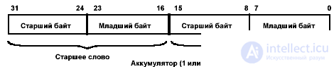
Batteries
These are general purpose registers for handling bytes, words, and double words. They are 32 bits in size.
The status word contains bits that you can refer to in operands of bit logic operations. The following sections explain the meanings of bits 0 through 8. Figure 1-6.
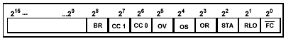
Change bits in the status word
| Value | Explanation |
| 0 | Sets the signal state to 0 |
| one | Sets the signal state to 1 |
| x | Changes state |
| - | Condition remains unchanged |
Bit 0 of the status word is called the primary interrogation bit (bit FC, see fig. 1.6). At the beginning of the LAD segment, the state of the FC bit signal is always 0, unless the previous segment has ended with the - (SAVE) command. (The bar above FC indicates that it is inverted, that is, the state of its signal at the beginning of the contact plan segment is always 0).
Each logical command polls the signal state of the FC bit and the contact to which this command is addressed. The signal state of the FC bit determines the sequence in which the logic chain is executed. If the FC bit is 0 (at the beginning of the LAD segment), the command saves the result in the result bit of the logical operation of the status word and sets the FC bit to 1. This process is called the primary poll. 1 or 0, stored after the initial poll in the RLO bit, then referred to as the result of the initial poll.
If the signal state of the FC bit is 1, then the operation logically matches the result of polling the signal state at the contact it processes with the previously formed RLO and stores this result in the RLO bit.
The sequence of commands of the contact plan (chain of logical operations) always ends with an output command (“Set Output”, “Reset Output”, “Output Coil”) or a transition command associated with the result of a logical operation. These commands reset the FC bit to 0.
Bit 1 of the status word is called the result bit of the logical operation (bit RLO, see Figure 2.6). This bit stores the result of a chain of bit logic or comparison operations. A change in the signal state of the RLO bit can provide information relating to the signal flow.
For example, the first command in the contact plan segment polls the signal state of the contact and returns a result of 1 or 0. This command stores the result of this signal state polling in the RLO bit. The second command in the chain of bit logic operations also polls the signal state of the contact and provides the result of the poll. The command then matches this result with the value stored in the RLO bit of the status word, in accordance with the principles of Boolean logic (see Primary Interrogation and Chapter 4 above). The result of this logical operation is stored in the RLO bit of the status word, replacing the previous value stored in the RLO bit. Each following command in the chain performs a logical operation with two values: the result obtained when polled by the contact command, and the current RLO value. For example, you can use a boolean bit logic command after initial polling to assign the state of the contents of a memory cell to an RLO bit or to trigger a transition.
Bit 2 of the status word is called the status bit (STA bit, see Figure 1-6). The status bit stores the value of the bit to which the call is made. The state of a bit instruction that has access to the memory for reading (“Normally Open Contact”, “Normally Closed Contact”) is always equal to the value of the bit that this operation polls (the bit with which it performs a logical operation). The state of the bit command that has access to the write memory (“Set Output”, “Reset Output”, “Output Coil”) is equal to the value of the bit to which the command writes, or, if no recording is made, to the value of the bit that the command refers to . The status bit does not matter for bit instructions that do not access memory. These commands set the status bit to 1 (STA = 1). The status bit is not polled by the command. It is analyzed only when testing a program (program status).
Bit 3 of the status word is called the OR bit (see Figure 1-6). The OR bit is required if you use the commands on the contacts to perform the logical AND operation before OR. Logical operations OR correspond to parallel connection of contacts. Logical operations And correspond to the sequential inclusion of contacts. The And function may contain the following commands: “Normally open contact” and “
Normally closed contact ”. The OR bit indicates to these operations that the previously executed AND function gave the value “1”, thereby anticipating the result of the logical OR operation. Any other instruction processing bits clears the OR bit.
Bit 5 of the status word is called the overflow bit (bit OV, see Figure 1-6). The OV bit indicates an error. It is set by an arithmetic operation or a comparison operation for floating-point numbers, after an error has occurred (overflow, invalid operation, invalid floating-point number). The bit is set (in case of an error) or reset in accordance with the result of an arithmetic operation or a comparison operation.
Bit 4 of the status word is called a persistent overflow bit (OS bit, see Figure 1-6). The OS bit is set with the OV bit when an error occurs. Since the OS bit remains set after the error is cleared (as opposed to the OV bit), it indicates whether an error occurred in one of the previously performed operations. The OS bit discards the following commands: JOS (Go after saved overflow,
STL programming), block calls and end of block.
Bits 7 and 6 of the status word are called condition code 1 and condition code 0 (CC 1 and CC 0, see fig. 2-6). CC 1 and CC 0 provide information on the following results or bits:
The following tables list the values of CC 1 and CC 0 after your program executes certain commands.
| CC 1 and CC 0 after arithmetic operations, without overflow | ||
| SS 1 | SS 0 | explanation |
| 0 | 0 | Result = 0 |
| 0 | one | Result <0 |
| one | 0 | Result> 0 |
| CC 1 and CC 0 after arithmetic operations with integers, with overflow | ||
| 0 | 0 | Overflow of negative domain when adding integers and double integers |
| 0 | one | Overflow of a negative domain with multiplication of integers and double integers Overflow of a positive region with addition and subtraction of integers, addition and subtraction of double integers, upon receipt of an addition to two integers and double integers |
| one | 0 | Overflow of a positive domain with multiplication of integers and double integers, with division of whole and double integers Overflow of a negative domain with addition and subtraction of integers, addition and subtraction of double integers |
| one | one | Dividing by 0 when dividing whole and double integers and when getting the remainder of dividing double integers |
| CC 1 and CC 0 after floating point arithmetic operations with overflow | ||
| 0 | 0 | Phased loss of significance |
| 0 | one | Negative area overflow |
| one | 0 | Positive overflow |
| one | one | Invalid operation |
| CC 1 and CC 0 after comparison operations | ||
| 0 | 0 | IN2 = IN1 |
| 0 | one | IN2 <IN1 |
| one | 0 | IN2> IN1 |
| one | one | IN1 or IN2 is an invalid floating point number |
| CC 1 and CC 0 after shift and cyclic shift operations | ||
| 0 | 0 | Last bit advanced = 0 |
| one | 0 | Last bit advanced = 1 |
| CC 1 and CC 0 after logical word operations | ||
| 0 | 0 | Result = 0 |
| one | 0 | Result <> 0 |
Bit 8 of the status word is called the bit of the binary result (the BR bit, see Figure 1-6). The BR bit forms the link between processing bits and words. This bit allows your program to interpret the result of an operation on words as a binary result and embed this result in a chain of binary logical operations. From this point of view, BR is an in-machine marker in which the RLO is stored before the RLO-modifying operation with words, so that the RLO remains available to continue the interrupted chain of bits after the operation has been completed.
For example, the BR bit allows you to program a function block (FB) or function (FC) in the command list (STL) and call this FB or this FC from the contact plan (LAD).
When you write a function block or function that you want to call from LAD, whether you write FB or FC to STL or LAD, you are responsible for manipulating the BR bit. The BR bit corresponds to the enable output (ENO) of the LAD block. You must store the RLO in the BR bit with the SAVE command (in STL) or with a coil --- (SAVE) (in LAD) according to the following criteria:
You must program these commands at the end of the FB or FC so that
they were executed as the last commands in the block.
The parameters of the enable input (EN) and the enable output (ENO) of the LAD unit operate in accordance with the following principles:
If you call a system function block (SFB) or a system function (SFC) in your program, the SFB or SFC indicates whether the CPU performed this function without errors or errors, providing the following information in the bit of the binary result:

Comments