
Lecture
ACOUSTOELECTRONIC INTERACTION (AEI) is the interaction of acoustic waves with conduction electrons in semiconductors and metals. The displacement of lattice atoms caused by an ultrasonic wave changes the intracrystalline fields, which affects the distribution and motion of the conduction electrons. In turn, the redistribution of the electrons and their directed motion alter the pattern of deformations and, consequently, the way acoustic waves propagate in the crystal.
Acoustoelectronic interaction (AEI) is a phenomenon in which acoustic waves interact with electrons in crystalline or semiconductor materials, changing their electrical properties. It is an important phenomenon with applications in various fields of science and technology. Here are some of them:
Acousto-optics: AEI is used in acousto-optic devices to change the properties of light waves. It is applied, for example, to create devices that control light intensity, modulate phase, and so on.
Acoustoelectronic filters: AEI is used in electronic filters to control the frequency of signals. It is used, for example, in radio systems for tuning or filtering signals.
Acoustoelectronic delay devices: AEI can be used to create signal delay devices, which are useful in radar and communications engineering.
Acoustoelectric resonators: Acoustoelectronic resonators can be used in radio receivers to select particular frequencies and amplify signals.
Materials research: Acoustoelectronic interaction is used in studying the properties of materials such as semiconductors, helping to understand their structure and characteristics.
These examples show how acoustoelectronic interaction plays an important role in creating various devices and technologies in science and engineering.
According to the current GOST standard, an acoustoelectronic product is an assembly unit that performs a certain function within radio-electronic equipment based on the processes of excitation, propagation, and conversion of acoustic waves in an elastic medium and (or) on their interaction with electromagnetic fields.
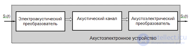
A generalized functional diagram of an acoustoelectronic device (AED) is shown in Fig. 1. The input electrical signal is converted by the input electroacoustic transducer into an acoustic wave propagating in the substrate of the device (the acoustic channel). The output acoustoelectronic transducer converts the acoustic wave into the output electrical signal. Information can be processed both in the acoustic channel and during the mutual conversion of electrical and acoustic signals. A distinctive feature of AEDs is the low propagation velocity of acoustic waves compared with electromagnetic waves. Information carriers in AEDs can be various types of acoustic waves: bulk waves, surface waves, and waves in material layers.
|
|
Fig. 1. Generalized functional diagram of an acoustoelectronic device
Today, many AEDs have been developed and are widely used. AEDs can be classified on the basis of various criteria, for example, functional purpose, functional complexity, adaptability, level and degree of integration, type of acoustic waves used, and design and topology (Fig. 2). By functional purpose, one distinguishes devices for signal generation and shaping, signal processing, object identification, measurement devices, and signaling devices. In terms of functional complexity, AEDs range from the simplest elements (adders, phase shifters, etc.) to acoustoelectronic processors that perform various signal processing operations, for example, the Fourier, Hilbert, and Mellin transforms, among others. By the type of acoustic waves used, the most widespread are devices based on surface, near-surface, and bulk acoustic waves (BAW), and less widespread are devices that use waves in material layers.
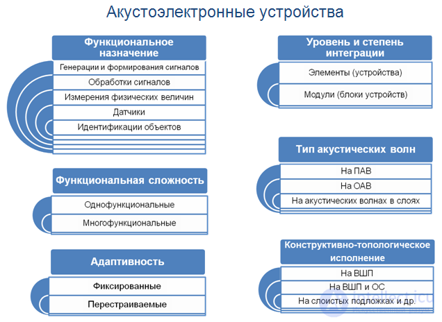
Fig. 2. Classification of acoustoelectronic devices
The principles of construction, description, and operation of AEDs are similar; the existing differences are related to the specifics of excitation, reception, and propagation of a particular type of acoustic wave. In SAW devices, the trend toward higher operating frequencies is associated with the observed shift in application from Rayleigh-type surface waves to leaky and pseudo-surface waves, which have higher propagation velocities and a number of other advantages. There are devices that simultaneously use several acoustic modes propagating in a single substrate and implement several functional operations.
In AEI, energy and momentum are exchanged between the ultrasonic wave and the conduction electrons. The transfer of energy from the wave to the electrons leads to additional electronic absorption of ultrasound, and the transfer of momentum leads to the acoustoelectric effect. When electrons in a conductor move in a directed manner at a supersonic velocity, they give up part of the energy of their directed motion to the wave, resulting in ultrasonic amplification. In addition, as a result of AEI, a number of specific mechanisms of nonlinearity of acoustic waves arise in conductors, giving rise to a variety of nonlinear effects.
AEI is the interaction of electrons with vibrations of the long-wavelength part of the acoustic spectrum ( , where T is the temperature and
  is the vibration frequency), in the description of which the crystal is treated as an elastic continuum and lattice vibrations are treated as waves of elastic deformation. In the high-frequency limit, AEI is equivalent to the electron-phonon interaction.
Mechanism of AEI. In the AEI process, the force F acting on free carriers from the deformed lattice induces electron currents and a redistribution of carriers. The electromagnetic fields that arise partially compensate the force F, and as a result of screening the force actually acting is smaller by a factor of  (
( is the dielectric constant of the crystal;
  are the frequency and wave vector of the ultrasonic wave). The redistributed charges and induced fields act on the lattice with a force whose volume density is ultimately proportional to the deformation amplitude. Depending on the type of crystal and the ultrasonic frequency range, the forces arising in the lattice-carrier system have different origins.
In semiconductors, AEI is determined by two main mechanisms. Common to all materials is the interaction via the deformation potential, caused by local changes in the band gap of the semiconductor under deformation. As a result, a force F proportional to the deformation gradient S acts on the electron:  with a deformation potential constant D, which depends on the propagation direction and polarization of the ultrasonic wave. In turn, a force proportional to the gradient of the carrier distribution function
  acts on the lattice:
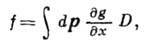
where p is the electron momentum, r is its position vector, and t is time. The interaction via the deformation potential grows with increasing ultrasonic frequency and is therefore effective at high frequencies in nonpolar semiconductors (Ge, Si, etc.) and semimetals (bismuth, etc.).
Piezoelectric interaction is observed in semiconductors lacking a center of symmetry: a deformation is accompanied by the appearance of an electric field and, conversely, an electric field causes deformation of the crystal. An electron in a sound wave experiences a force
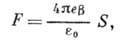
proportional to the strain (e is the electron charge,  is the piezoelectric modulus,
  is the dielectric permittivity of the lattice). The body force acting on the lattice is proportional to the gradient of the electric field
  induced by the ultrasonic wave:
 .
.
The strong anisotropy of the piezoelectric effect makes the acoustoelectronic interaction (AEI) depend on the propagation direction and polarization of the ultrasonic wave. Piezoelectric interaction is the main AEI mechanism in piezoelectric semiconductors (CdS, ZnO, GaAs, InSb, Te, etc.) up to frequencies of the order of 10-100 GHz, above which interaction via the deformation potential becomes dominant. In a number of centrosymmetric crystals — ferroelectrics (SbSI, BaTiO3, etc.) — owing to the electrostriction effect and large internal electric fields Eint, an AEI arises that formally reduces to the piezoelectric one. In this case the effective piezoelectric constant is 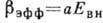 , where a is the electrostriction constant.
In metals, because of the high electron concentration, the electrons, along with the ionic lattice, determine the elastic properties of the material. The AEI arises as a result of the action on the electrons and lattice ions of a self-consistent electromagnetic field produced by the motion of the ions. For longitudinal sound this field is electrostatic in nature; in the case of transverse sound, a vortex electric field acts on the electrons and ions. Along with the forces determined by the macroscopic electromagnetic field of the sound wave, the electrons are also acted upon by forces due to the local change of the electron dispersion law upon deformation of the crystal. Since only a small number of electrons belonging to the Fermi surface interact effectively with the sound wave, this interaction is determined by the deformation potential, which describes the local perturbation of the Fermi surface. Quite often, especially in the quantum-mechanical description of the AEI in metals, the whole interaction is described in terms of an effective deformation potential. The electromagnetic interaction mechanism manifests itself, besides in metals, in semimetals and in semiconductors whose lattice contains a large number of charged impurities.
In crystals with a pronounced magnetostriction effect, an AEI is possible that is due to an alternating magnetic field proportional to the strain. It is characteristic of ferromagnetic metals (nickel, cobalt) and alloys, as well as other magnetic materials, and depends on the spontaneous magnetization and the strength of the external magnetic field.
Screening. The efficiency of the AEI is determined not only by the magnitude of the forces acting on the electrons, but also by the way the electron subsystem rearranges under the action of these forces. As a result of screening, AEI effects depend on the high-frequency electronic conductivity — the response of the electrons to the alternating and inhomogeneous electric field induced by the ultrasound. The dependence of the conductivity on frequency, external electric and magnetic fields, and temperature shows up in the acoustic characteristics of the conductor.
Screening leads to a complex frequency dependence of the AEI. Its character is determined by the ratio between the acoustic wavelength  and the electron mean free path
 . If an electron undergoes a large number of collisions over a wavelength (kle=
  ), the acoustic wave interacts with electron bunches — perturbations of the electron density. The behavior of the electron gas in this case is well described by the hydrodynamic equations. It is in this frequency range that the relaxation character of the screening process shows up: the degree of screening depends on the ratio between the oscillation period and the electron relaxation time
  (
( is the static conductivity).
At  the external force is screened almost completely. As the frequency increases, the degree of screening decreases, but at the same time the wavelength — the characteristic distance over which the external force acts — also decreases. Therefore, at high frequencies, when l becomes smaller than the spatial screening scale — the Debye–Hückel radius
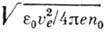 (
( is the thermal velocity of the electron, n0 is the electron density), the degree of screening is again large. Minimum screening occurs at krD=1.
When the mean free path is long (kle>l), the acoustic wave interacts with individual electrons. The main contribution to the AEI comes from a small group of electrons moving in phase with the wave, whose velocity component u along the wave propagation direction is close to the speed of sound  . For the remaining electrons the interaction with the wave is ineffective, since over the mean free path the force acting on them changes sign many times.
Effects of the acoustoelectronic interaction. In experiments the AEI shows up either directly as the effect of drag of charge carriers by the acoustic wave, or as a dependence of the acoustic wave parameters (its velocity, absorption coefficient, etc.) on the concentration of conduction carriers and on the magnitude of external electric and magnetic fields. The AEI is one of the causes of sound dispersion in solids. Having gained energy in the AEI process, the electrons dissipate it in collisions with defects and thermal phonons, giving rise to electronic absorption of ultrasound. The frequency dependence of the absorption coefficient may then differ from the quadratic one predicted by classical theory (see Sound absorption ). In semiconductors in a strong electric field, sound absorption gives way to sound amplification. Amplification of low-frequency phonons (acoustic noise) by the electric field leads to the development of an electrical instability in semiconductors and to the formation of acoustoelectric domains. The AEI is a source of electronic acoustic nonlinearity, which makes the amplitudes of acoustic waves arising from nonlinear interaction depend on electronic parameters, and which gives rise to electroacoustic echo effects in semiconductors, etc.
Electronic absorption of ultrasound in metals is dominant at low temperatures. In the long-wavelength region  the electronic absorption is due to the viscosity of the electron gas; the absorption coefficient
  is then proportional to the time
 between electron collisions and to the square of the frequency:
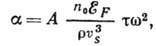
where  is the Fermi energy,
 is the density of the metal,
  is the speed of sound, A is a numerical coefficient . The temperature dependence of the electronic absorption is determined by the dependence
  . As the temperature decreases, the time between collisions increases, and the electronic absorption grows with it. In the short-wavelength region
  the absorption coefficient increases linearly with frequency
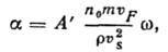
where is the Fermi velocity of the electron, m is its mass, and
 is a numerical coefficient. The absorption coefficient
 contains no dependence on
  , and therefore does not depend on the carrier scattering mechanism and depends only weakly on temperature.
Acoustic absorption in metals placed in a constant magnetic field has a special character. In a magnetic field the electron trajectories are curved, and in sufficiently strong fields, for which the cyclotron frequency  (B is the magnetic induction, c is the speed of light) greatly exceeds the collision frequency
 , the motion becomes periodic. The trajectories of such motion are determined by the topology of the Fermi surface.
In the general case the absorption coefficient is of the same order as in the absence of the field. However, when an integer number of wavelengths fits along the characteristic size of the electron trajectory (the orbit diameter for closed trajectories or the spatial period for open ones), the absorption increases sharply. As a result, the absorption coefficient exhibits an oscillatory dependence on frequency or magnetic field: the interaction of the wave with electrons on closed trajectories gives rise to geometric oscillations, and on open trajectories, to magnetoacoustic resonance. At low temperatures in strong magnetic fields quantum oscillations arise, a periodic dependence of the ultrasonic absorption coefficient on 1/B (Fig. 1), caused by the quantization of electron motion in a magnetic field (see Quantum oscillations in a magnetic field). In origin, quantum oscillations of ultrasonic absorption are analogous to the Shubnikov–de Haas effect. Finally, at ωτ > 1 acoustic cyclotron resonance can be observed.
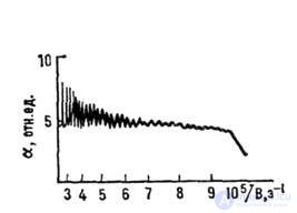
Fig. 1. Giant quantum oscillations of the ultrasonic absorption coefficient in zinc at a frequency of 220 MHz and T = 4.2 K.
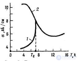
Fig. 2. Temperature dependence of the absorption coefficient of longitudinal sound waves in lead at a frequency of 50 MHz: 1 - in the superconducting state; 2 - with superconductivity destroyed by a magnetic field.
Acoustic absorption in superconductors occurs only because of the interaction of the acoustic wave with "normal" electrons; superconducting electrons do not participate in sound absorption. Since the number of "normal" electrons decreases with decreasing temperature, at a temperature T<Tc (Tc is the superconducting transition temperature) the sound absorption coefficient falls, tending to zero at  (Fig. 2, curve 1).
Electronic absorption of ultrasound in semiconductors is the main absorption mechanism over a wide range of temperatures and frequencies. Several mechanisms of acoustoelectronic interaction (AEI), the presence of different types of carriers and impurity centers, the possibility of varying the concentration and mobility, and the influence of electric and magnetic fields lead to a complex picture of acoustic absorption in semiconductors. In piezoelectric semiconductors, the piezoelectric AEI mechanism dominates over all others at temperatures up to room temperature and in the frequency range up to tens of Hz, and makes the main contribution to absorption compared with other mechanisms of acoustic energy dissipation. For room temperatures, when the electron mean free path is much smaller than the wavelength, the absorption coefficient has the form

where is the electromechanical coupling coefficient.
At low temperatures, when  , the absorption coefficient
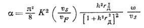
does not depend on the time between collisions  , and therefore depends only weakly on temperature. In both cases the absorption grows with increasing frequency and the coefficient
  reaches a maximum equal to , at
  (Fig. 3, curve 1), and then
  decreases due to Coulomb screening. The latter also determines the dependence of the absorption coefficient on the carrier concentration n0: it first grows in proportion to n0, and then, passing through a maximum, falls as 1/n0. For all reasonable carrier concentrations, ultrasonic absorption in piezoelectric semiconductors is considerably more effective at
  , i.e., in the room-temperature region.
Significant electronic absorption due to AEI via the deformation potential is observed in many-valley semiconductors (Ge, Si) and semimetals (Bi), where the electron energy has several minima (valleys) located at different points of the Brillouin zone.
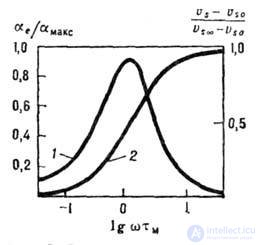
Fig. 3. Dependence of the electronic ultrasonic absorption coefficient (1)  and of the change in sound velocity (2) on the quantity
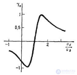
Fig. 4. Dependence of the electronic ultrasonic gain coefficient  on the electron drift velocity
For a given wave propagation direction, forces equal in magnitude but opposite in direction will act, owing to AEI, on electrons belonging to two different minima. Then no inhomogeneous space charge is formed and the screening is weak. The absorption coefficient in this case grows monotonically with increasing n0 and in crystals with a high concentration reaches a significant value.
In strong magnetic fields at low temperatures, the same resonance oscillatory dependences as in metals are observed in degenerate semiconductors and semimetals. In nondegenerate semiconductors only acoustic cyclotron resonance can be observed.
Electronic dispersion of the sound velocity is most significant in piezoelectric semiconductors, where it reaches several percent. The dispersion is of a relaxation nature: at low frequencies the electrons almost completely screen the piezoelectric fields, and the sound velocity equals the value vsq, determined only by the elastic properties of the crystal. At high frequencies  the influence of electrons is negligible and the sound velocity equals its value in a piezoelectric dielectric
 (Fig. 3, curve 2).
Amplification of ultrasound in semiconductors arises when there is a directed motion (drift) of charge carriers along the direction of wave propagation. The drift is created by an external electric field. As the field increases, the motion of the electrons first reduces the absorption coefficient (Fig. 4), and then, when the drift velocity  equals
  , reduces it to zero. With supersonic motion
  electronic amplification of ultrasound arises; it occurs at the expense of the energy of the source maintaining the supersonic drift of the carriers. As the strength of the external field increases, the gain grows linearly, reaches a maximum, and then begins to decrease, because at high drift velocities the electrons do not have time to interact effectively with the sound wave (Fig. 4). In piezoelectric semiconductors at
  the electronic gain coefficient
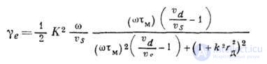
reaches a maximum equal to 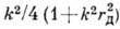 , at a drift velocity of

fairly close to  . In the case
  the dependence
  remains linear up to values
 , close to the thermal (or Fermi) velocity of the electrons
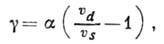
where  is the electronic absorption coefficient in the absence of drift.
Amplification of ultrasound is possible only if it exceeds the absorption caused by the lattice. Ultrasound amplification has been observed experimentally in piezoelectric semiconductors (CdS, CdSe, Te, GaAs, InSb, etc.) in the frequency range 10-104 MHz at temperatures from liquid-helium to room temperature. The experimentally observed gain increments are 20-80 dB/cm. At low temperatures, ultrasound amplification has also been observed in nonpolar semiconductors (Ge) and semimetals (Bi).
Electronic acoustic nonlinearity. The effects considered above relate to the propagation of sufficiently weak ultrasound. As the intensity of the sound wave increases, nonlinear effects play an ever greater role, distorting its shape, limiting the growth of its intensity during amplification, or reducing its attenuation. In conducting media, in addition to the usual lattice anharmonicity, there is a specific nonlinearity mechanism associated with the trapping of conduction electrons in the minima of the potential energy of the electric field accompanying the acoustic wave (so-called electronic acoustic nonlinearity). In semiconductors this nonlinearity mechanism becomes significant at ultrasound intensities much lower than those at which the lattice anharmonicity characteristic of dielectrics comes into play. The trapping of electrons by the electric field of the wave leads to different effects depending on the ratio between the sound wavelength and the electron mean free path.
For low-frequency sound  in piezoelectric semiconductors, the main role is played by the spatial redistribution of carriers: as the sound intensity increases, the number of electrons trapped in the potential wells created by the alternating piezopotential
  grows (so-called concentration nonlinearity). When the depth of the potential wells -
 exceeds the thermal energy of the electrons kT, the carriers become stuck in the wells and have less effect on the wave. As a result, the electronic amplification (absorption) of sound decreases with increasing intensity, and the waveform differs substantially from sinusoidal.
During the propagation of high-frequency sound  in metals, semimetals and semiconductors, the acoustic wave strongly distorts the momentum distribution of those electrons that move in phase with the wave and interact effectively with it (so-called momentum acoustic nonlinearity). This distortion is stronger the greater the sound intensity, and the longer the time between collisions, which determines the lifetime of an electron in a potential well.
As the intensity increases, more and more electrons move in phase with the wave and do not interact with it, which leads to a decrease in the amplification or absorption of sound. Momentum acoustic nonlinearity is analogous to nonlinear Landau damping of electromagnetic waves in a plasma. There are also a number of other electronic mechanisms of acoustic nonlinearity, associated, for example, with heating of the electron gas by the ultrasonic wave, trapping of carriers at impurity centers (traps), etc.
Owing to electronic acoustic nonlinearity, when an ultrasonic wave propagates in a crystal, electric fields and currents arise not only at the ultrasound frequency but also at harmonic frequencies. The back action of these fields on the lattice leads to the generation of acoustic harmonics. Similarly, when several ultrasonic waves propagate simultaneously in a crystal, electronic nonlinearity causes nonlinear interaction of acoustic waves (see Nonlinear acoustics ). When a crystal is subjected to an alternating electric (electromagnetic) field, electronic nonlinearity provides parametric amplification of acoustic waves at subharmonics of the external field frequency, the effect of acoustic wavefront reversal, which underlies electroacoustic echo, and other effects.
Acoustoelectronic interaction effects in semiconductors are used in acoustoelectronics to create devices for amplifying and generating waves, controlling the amplitude and phase of a wave, and performing nonlinear operations on signals. Acoustoelectronic interaction in metals is widely used to study the shape of the Fermi surface.
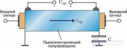
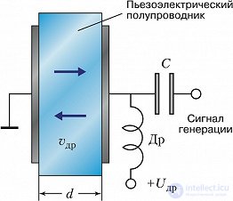
The interaction of acoustic waves with conduction electrons in solids leads to phenomena such as electronic amplification and absorption of acoustic waves and the acoustoelectric effect, which underlie the operation of acoustoelectronic amplifiers, generators, phase shifters, etc. In acoustoelectronic BAW amplifiers (Fig. 5), the amplification of waves occurs as a result of their interaction with drifting charge carriers in the volume of a bulk bar of piezoelectric semiconductor. To create carrier drift, an electric voltage (so-called drift voltage) is applied to the end faces of the bar, producing a drift current of electrons. In continuous operation, the drift current can lead to overheating of the amplifier and cause its destruction. When the amplifier operates in pulsed mode, the drift voltage is applied as pulses whose duration equals the transit time of the amplified signal through the acoustic delay line; in this case the average dissipated power is relatively low. The operation of the acoustoelectronic BAW generator is based on the electronic amplification effect; it is an acoustic resonator made as a piezoelectric semiconductor plate with electrodes deposited on its end faces (Fig. 6). If the propagation direction of acoustic waves in the acoustic resonator coincides with the direction of carrier drift, they are amplified. At a sufficiently high drift velocity, the energy gain from the amplification of acoustic waves exceeds the losses associated with the absorption of waves propagating in the opposite direction and with their reflections from the faces of the resonator, which leads to the generation of acoustic oscillations. The amplitude and frequency spectrum of the generated oscillations are determined mainly by the carrier concentration and the plate thickness.
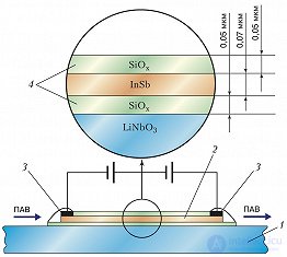
Among SAW devices, the most promising are acoustoelectronic SAW amplifiers based on monolithic layered structures containing a "strong" piezoelectric (e.g., LiNbO3), in which the SAW propagates, and a thin semiconductor film with high electron mobility (e.g., of InSb), in which the charge carriers drift (Fig. 7). The interaction of the SAW with drifting charge carriers takes place in the semiconductor film, into which the alternating electric field accompanying the SAW penetrates. The use of layered structures makes it possible to obtain continuous SAW amplification, as well as suppression of spurious signals caused by reflection of the SAW from the crystal ends and from the transducers. The gain of such an amplifier reaches 30–60 dB/cm at a noise figure of less than 10 dB in the frequency range from 100 to 500 MHz (with a bandwidth of 5–20%).
A device whose operating principle relies on the dependence of the acoustic wave velocity on the parameters of the electronic subsystem in a semiconductor is the acoustoelectronic SAW phase shifter. To change the phase of electromagnetic oscillations, they are converted into acoustic waves and back, and in the process the velocity of the acoustic waves along their propagation path is influenced, and hence the phase of the acoustic oscillations registered by the output transducer. For example, by controlling the conductivity of a photosensitive semiconductor film deposited on the surface of a piezoelectric acoustic medium (by varying the illumination intensity or the electron drift velocity), the SAW propagation velocity can be controlled.
The potential difference that arises due to the acoustoelectric effect at the boundaries of a piezoelectric semiconductor or of a semiconductor layer in a piezoelectric–semiconductor structure is used in so-called square-law or synchronous acoustoelectric detectors of acoustic waves. These devices, which have a wide dynamic range, have become widespread in acoustoelectronic signal processing devices.
Applications of SAW Acoustoelectronic Components
Today, SAW technologies and SAW components have firmly established their niche in electronic equipment of various kinds.
All applications can be divided into two main areas: the first is consumer electronics, and the second is special-purpose and professional electronics. On closer examination, the following most important applications can be singled out:
The Global Market of SAW Acoustoelectronic Components
Currently, more than 50 companies worldwide are engaged in the development and production of SAW acoustoelectronic components. They include both large multinational companies with offices in various countries that carry out large-scale production of a wide range of devices, and small firms with small-scale production. The largest manufacturers are Epcos, Murata, Vectron International, RF Monolithics, and TriQuint. Table 2 lists some manufacturers of SAW components and the range of products they offer.
Table 2. SAW device manufacturers
|
Company (country) |
Products |
|
Vectron International |
F, R, O, S |
|
RF Monolithics, Inc. |
F, R, O, M |
|
Epcos |
F, AD, M |
|
NDK (NIHON DEMPA KOGYO) Co., Ltd. |
F, AD |
|
Murata Manufacturing Co., Ltd. |
F, AD |
|
Vanlong (China) |
F, R |
|
Amplitronix |
F, R |
|
Abracon Corporation (USA) |
F, R |
|
Phonon corporation |
F, AD, R, DL, C, O |
|
RFSAW, Inc. |
S, RFID |
|
SAWcomponents (Germany) |
F, R, S, RFID |
|
Panasonic Corporation |
F, AD |
|
API Technologies Corporation (USA) |
O, F |
|
Rakon (New Zealand) |
DL, M |
|
ECS Inc. International (USA) |
R |
|
ASR&D Corporation (USA) |
S |
|
CTS Corporation |
O |
|
Senseor (France) |
S |
|
Shoulder Electronics Ltd. (China) |
F, R |
|
AEK Design (Russia) |
F, R, S, DL |
Note. Legend: F – filter, R – resonator, AD – antenna duplexer, M – module, DL – delay line, C – correlator, O – oscillator, S – sensors, RFID – radio-frequency identification devices.

Comments