
Lecture 18 min.
The optical range of the electromagnetic wave spectrum occupies the wavelength interval from 1 mm to 1 nm, lying between microwave electromagnetic waves and soft X-rays (Fig. 1).
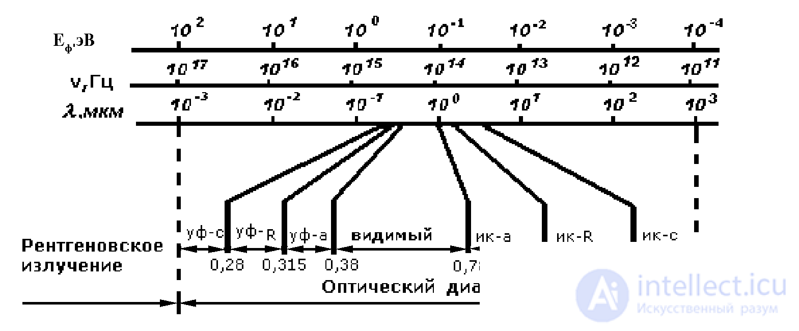
Fig. 1
It includes three sub-ranges, namely:
ultraviolet, UV (UV-A, UV-B, UV-C), corresponding to wavelengths of 1 nm - 0.38 μm;
visible, corresponding to wavelengths of 0.38 - 0.78 μm;
infrared, IR (IR-A, IR-B, IR-C), corresponding to wavelengths of 0.78 μm - 1 mm.
The wide exploitation of the optical range is determined by a number of fundamental advantages of light waves over radio waves.
The working range of semiconductor devices is the region of wavelengths of 0.2 - 20 μm.
When optical radiation interacts with a semiconductor crystal, it is partly absorbed, partly reflected from its surface, or passes through the crystal without absorption. The fractions of transmitted, reflected and absorbed radiation energy are estimated for semiconductor materials by the corresponding coefficients. One distinguishes:
- The transmittance Tph - the ratio of the power Ptr transmitted through the semiconductor crystal to the power Pin of the radiation incident on its surface;
- The reflectance Rph - the ratio of the power Prefl reflected from the crystal surface to the incident power Pin;
- The absorption coefficient α (cm-1), numerically equal to the reciprocal of the distance from the semiconductor surface over which the initial power of the incident radiation decreases by a factor of e, where e is the base of the natural logarithm. The absorption coefficient α is the decay constant of the radiation power along the coordinate x directed into the semiconductor, normal to its surface, i.e. dP/dx = - αP. Then
P(x) = Pin(0) exp(-αx) (1)
where Pin(0) is the power of the radiation incident on the semiconductor surface.
In photometry, radiation power is expressed through the luminous flux or radiant flux Φ (lm). The two quantities P and Φ are related through a characteristic that takes into account the peculiarities of perception of radiation by the human eye at each wavelength λ and is called the spectral luminous efficacy, i.e. S* = Φ/P. Then from (1), after multiplying by S*, we obtain:
Φ(x) = Φin(0) exp(-αx) (2)
The number of photons incident on a unit surface of the semiconductor per second in a monochromatic light flux is called the photon density N0. Taking the density into account, the luminous flux is written as Φ = hνN0, where h is Planck's constant (J·s) and ν is the frequency (Hz). The light flux interacting with the crystal, taking the reflectance Rph into account, we define as Φ(x) = (1-Rph)N0hν exp(-αx). The change in photon density with depth x is found from the expression:
dN/dx = -(1-Rph)N0 α exp(-αx), (3)
where the sign « - » indicates that the photon density decreases with depth x because of absorption.
The dependence of the absorption coefficient on the radiation wavelength (frequency, quantum energy) is called the absorption spectrum. A typical absorption spectrum of a semiconductor α = f(λ) is shown in Fig. 2 (only the infrared part of the range is shown. As the wavelength decreases further, α remains unchanged - solid line). Individual regions of the spectrum with local maxima of the absorption coefficient correspond to different mechanisms of absorption of radiation energy in semiconductors. The energy absorption mechanisms will be considered below.
Radiation reflected from the crystal surface is excluded from the interaction with the semiconductor. In photoelectric devices one tries to reduce the fraction of reflected energy by decreasing the reflectance, and to increase the fraction of absorbed energy by increasing the absorption coefficient, since only absorbed energy causes generation of free carriers in semiconductors. One way to reduce the reflectance consists in changing the conditions of reflection of the electromagnetic wave from the crystal surface. For this purpose one or several layers of an antireflection coating are deposited on the crystal surface.
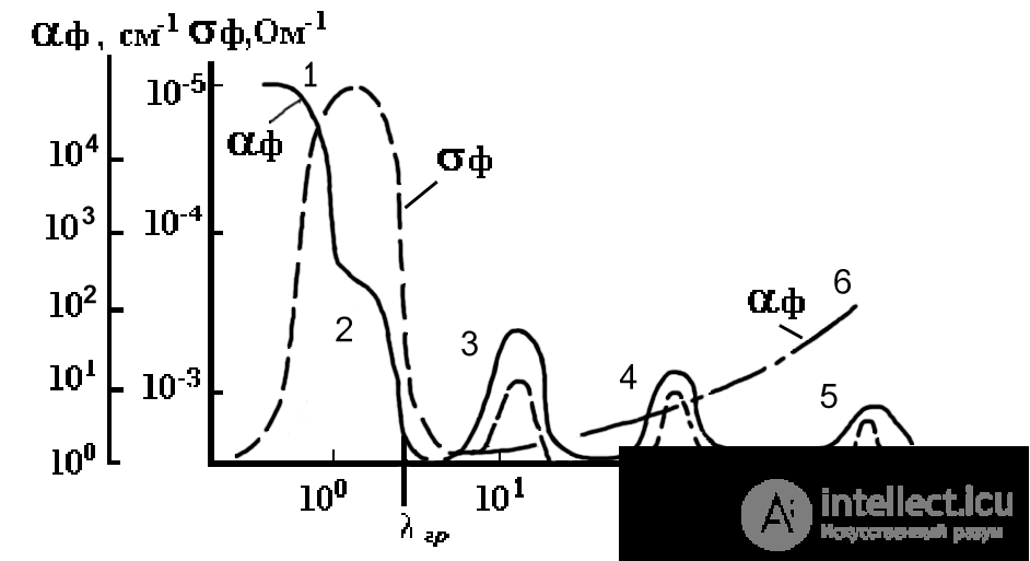
Fig. 2
In semiconductors one distinguishes several mechanisms of radiation energy absorption - intrinsic (fundamental, interband), impurity, exciton, lattice absorption, and absorption by free carriers.
In intrinsic absorption the energy is spent on breaking a valence bond in an atom and transferring an electron from the valence band of the semiconductor to the conduction band. This process of free carrier generation is the reverse of interband recombination. To transfer an electron to the conduction band, the photon energy must exceed the band gap, i.e. Eph = hν ≥ Eg. At radiation frequencies ν < νb, where νb = Eg/h, the absorption coefficient decreases sharply. Therefore the intrinsic absorption spectrum has a well-defined edge, called the red limit of the photoelectric effect and determined by the relation λb = ch/Eg (Fig. 2). The red limit corresponds to the minimum photon energy needed to transfer an electron from the valence band to the conduction band (the ionization energy of the semiconductor's own atom). One distinguishes direct and indirect transitions of electrons from the valence band to the conduction band. As the radiation wavelength decreases in the region of λb, indirect transitions may first be observed, in which a lower photon energy is required to ionize the atom (region 2 in Fig. 2), and then, as the photon energy grows, only direct transitions occur (region 1), since the probability of indirect transitions is already small. In region 1 of the absorption spectrum the values are α ~ 105-108 cm-1. The intrinsic absorption edge λb = c/νb of most semiconductors falls in the visible or infrared part of the optical range. The value of λb depends, besides the type of semiconductor, on temperature, external fields, doping level, etc. As temperature increases, the band gap of most semiconductors decreases and λb shifts toward longer wavelengths. As the impurity concentration in semiconductors increases, the energy levels near the top of the valence band or the bottom of the conduction band become filled. Therefore, in intrinsic absorption, where the photon energy must exceed the band gap, λb correspondingly shifts toward shorter wavelengths. In an electric field the red limit λb shifts toward the long-wavelength region (the Keldysh-Franz effect), and in a magnetic field, toward the short-wavelength region (Landau splitting).
In impurity absorption the photon energy is spent on ionizing impurity atoms. In semiconductors donor impurities are located near the bottom of the conduction band, and acceptor impurities near the top of the valence band. In both cases the impurity ionization energy is Ei << Eg, and the impurity absorption coefficient is several orders of magnitude smaller than the intrinsic one and does not exceed α = 103 cm-1. The impurity absorption spectrum is shifted toward the infrared region relative to the intrinsic absorption spectrum. Electrons in impurity atoms can be in the ground and excited states, and then the ionization energies of the impurity atoms differ. Therefore the impurity absorption spectrum consists of several regions (regions 3 and 4). Increasing temperature promotes thermal ionization of impurity atoms. The impurity absorption coefficient then decreases, since the photon energy is not absorbed owing to the absence of un-ionized impurity atoms. Therefore infrared detectors that use impurity absorption are, as a rule, cooled to low temperatures (77, 110 K).
In exciton absorption the photon energy is Eph < Eg. An electron in the valence band of the semiconductor, having absorbed the photon energy, does not detach from the atom but only passes into an excited state, forming with a hole a pair bound by Coulomb forces - an exciton. The exciton is electrically neutral, and its energy state corresponds to an energy level in the band gap of the semiconductor. The influence of the exciton on the conductivity of the semiconductor is indirect. A collision of the exciton with a photon or phonon can lead to its loss of energy, which is equivalent to the electron returning to an energy level in the valence band, or to its gaining energy, in which case the electron passes into the conduction band. In both cases the exciton decays. The exciton absorption spectrum consists of narrow lines in the region of λb (not shown in Fig. 2), but for each line λ > λb.
Semiconductors whose crystal lattice contains atoms of different types can be regarded as a system of electric dipoles. The dipoles absorb radiation energy most intensely at their natural vibration frequencies. The vibrations of the dipoles are complex, and therefore the lattice absorption spectrum consists of several regions. In Fig. 2, lattice absorption corresponds to region 5, in the far-infrared part of the optical range. The absorption is accompanied by the generation of a large number of phonons. The thermal energy of the semiconductor increases, the mobility and energy of free carriers change, and their concentration rises.
The absorption of energy by free carriers is associated with their transitions to levels within the conduction band. Because of the small energy gap between the levels of the band, the absorption spectrum is practically continuous (line 6 in Fig. 2) and is shifted toward the long-wavelength region of the optical range. In complex semiconductors, transitions of carriers between valleys correspond to peaks in the absorption spectrum.
In addition to those mentioned, other absorption mechanisms also occur in semiconductors, but their contribution to the photoconductivity of semiconductors is small. Thus, the photoresistive effect consists in a change in the electrical conductivity of a semiconductor under the action of radiation. The dark conductivity of a semiconductor at zero luminous flux F=0 and constant temperature is determined by the relation o=q(non+pop), where no, po are the equilibrium concentrations of electrons and holes; n, p are their mobilities. When radiation is absorbed in the semiconductor, excess carriers are generated. At constant values of the luminous flux FO, and of the carrier mobility and lifetime, full dynamic equilibrium is established in the semiconductor, with excess carrier concentrations n and p. The conductivity of the semiconductor changes by the amount:
f=q(nn+pp), (4)
called the photoconductivity. The total conductivity of the semiconductor is =o+f. The spectral characteristic of the photoconductivity f=() is shown in Fig. 2 by the dashed line.
The concentrations of nonequilibrium carriers that determine the photoconductivity depend on the parameters of the semiconductor (band gap width, conductivity type, refractive index, etc.) and on the absorption mechanism.
In the case of intrinsic absorption, a decrease in the radiation wavelength starting from the red limit of the photoelectric effect (see Fig. 2) leads to a sharp increase in photoconductivity, whose value passes through a maximum and then falls. The cause of this decrease in photoconductivity is a change in the region where free carriers are generated in the semiconductor. As the wavelength shortens, the carrier generation region moves into a rapidly narrowing surface layer of the semiconductor, where the main part of the radiation energy is absorbed (f increases). Because of surface phenomena in the semiconductor, the recombination rate of nonequilibrium carriers increases and their lifetime decreases, so the surface layer cannot make a noticeable contribution to the total conductivity of a thick semiconductor. With intrinsic absorption, carriers are generated in pairs, so the concentrations of excess carriers are equal, i.e. p=n. The photoconductivity of a semiconductor with intrinsic absorption is called bipolar (intrinsic). In wide-gap undoped semiconductors, the concentration of excess carriers exceeds the intrinsic concentration, i.e. n>no, p>po; in narrow-gap semiconductors, because of thermal generation, no, po.
In semiconductors with impurity absorption, the concentration of carriers of only one sign increases - either majority or minority carriers - and the photoconductivity is accordingly called unipolar (extrinsic). It corresponds to regions 3 and 4 (dashed lines) of the absorption spectrum in Fig. 2.
The absorption of energy by free carriers does not change their concentration but increases their mobility. Accordingly, with this absorption mechanism the photoconductivity is called - photoconductivity. At normal temperature, free carriers give up the absorbed energy to the lattice after 10-10 - 10-12 s, the lifetime of excited carriers. Therefore - photoconductivity is observed only at low temperatures (77, 110 K).
The efficiency of absorption is estimated by the quantum yield of the semiconductor f - the ratio of the number of nonequilibrium excess carriers produced in it to the number of absorbed photons.
To increase the photoconductivity of a semiconductor (extrinsic or intrinsic), it is necessary to increase the absorption coefficient (only for a thin semiconductor, where fL<<1, and L is the thickness), the quantum yield, and the carrier lifetime, and to reduce the reflection coefficient.
Photoelectric effects in an electrical junction.
Consider an idealized p-n junction irradiated by a monochromatic luminous flux with a photon energy exceeding the band gap of the semiconductors. With intrinsic absorption, excess carriers - electrons and holes - are optically generated in the junction and in the regions adjacent to it. The electric field of the junction moves holes into the p-region and electrons into the n-region, thereby separating the generated carriers. The carriers subject to separation are those generated in the depletion region of the junction and in the adjacent regions whose size is approximately equal to the diffusion length of minority carriers. Only from a distance shorter than the diffusion length can a minority carrier, while moving, manage to cross the junction boundary within its lifetime. Minority carriers generated in the p- and n-regions at a greater distance from the junction boundary do not reach the depletion region, where the electric field of the junction is concentrated, because of recombination.
A drift photocurrent of nonequilibrium minority carriers flows through the junction. Nonequilibrium majority carriers cannot overcome the potential barrier of the junction and remain in the generation region. As a result of the separation of optically generated carriers, the concentrations of holes in the p-region and of electrons in the n-region increase, which leads to compensation of the space charge of the immobile impurity ions at the junction boundaries. The potential barrier of the junction, as under forward voltage, is reduced by the value of the photo-EMF, called the open-circuit voltage Uoc when the external circuit is open. The lowering of the potential barrier increases the diffusion current of majority carriers through the junction. It is directed opposite to the photocurrent. In the steady state at F=const, the diffusion current Idf is equal to the drift current, which consists of the photocurrent If and the thermal current Io of the junction, i.e. the condition of dynamic equilibrium is satisfied:
I=Idf-If-Io=0 (5)
In an idealized p-n junction, the diffusion current and the thermal current are related by Idf=Ioexp(Uoc/T). Then from condition (5) it follows that
If=Io(eUoc/T-1) (6)
This formula for the open-circuit voltage can be written in the form:
Uoc=Tln(1+If/Io) (7)
The open-circuit voltage cannot exceed the contact potential difference of the p-n junction o. Otherwise, because of complete compensation of the field in the junction, the separation of optically generated carriers by the junction field stops. For nondegenerate semiconductors, the quantity qo is less than the band gap of the semiconductor. Therefore the inequality Uoc=o<Eg/q holds for the open-circuit voltage.
The photocurrent is directly proportional to the concentrations of nonequilibrium carriers generated per unit time in a region of size L+Lp+Ln, where L is the thickness of the junction and Lp and Ln are the diffusion lengths of minority carriers. These concentrations are directly proportional to the value of the monochromatic luminous flux. Therefore the luminous flux and the photocurrent are related by a linear dependence.
At low luminous fluxes, If/Io<1. Expanding function (7) in a series and discarding the small higher-order terms, we obtain Uoc = TIf/Io, i.e. in this case the open-circuit voltage is proportional to the luminous flux. At high luminous fluxes, If/Io>>1. The unity in relation (7) can be neglected compared with the ratio If/Io. Then, as the luminous flux grows, the open-circuit voltage increases according to a logarithmic law.
Energy diagrams of an unilluminated and an illuminated electrical junction are shown in Fig. 3.a, b. The luminous flux in an open-circuited p-n junction shifts the Fermi levels in the p- and n-regions by the amount qUoc because of the increase in carrier concentration due to nonequilibrium carriers, and the potential barrier of the junction is lowered.
When the illuminated p-n junction is short-circuited, a short-circuit photocurrent appears in the external circuit:
If=Isc=qSG(L+Lp+Ln), (8)
where S is the junction area; G is the generation rate of nonequilibrium carriers.
If the junction thickness L is much smaller than the diffusion length of minority carriers Ln or Lp, then the photocurrent is Isc = qGS(Ln+Lp). When the junction is short-circuited (Fig. 3.c), the carriers generated by light create the current Isc in the external circuit and do not compensate the charge of the ions near the junction boundaries, so the potential barriers of the illuminated and unilluminated junctions coincide in value.
Connecting a load resistor Rl (Fig. 3.d) to the illuminated junction reduces the current in the external circuit, i.e. Il < Isc, which means that not all optically generated carriers can be removed from the p- and n-regions by this current. Therefore a photo-EMF arises in the junction, whose value is less than the open-circuit voltage. The photo-EMF and the voltage across the load must be equal, and equal to Ul=IlRl, where at F=const the current in the external circuit is
Il = If+Io-Idf. (9)
In the new dynamic equilibrium the potential barrier of the junction is lowered by Ul, and a diffusion current Idf=Ioexp(Ul/T) flows through the junction. Then from condition (9) it follows that If-Il=Io[exp(Ul/T)-1], or
Ul=Tln[1+(If-Il)/Io]. (10)
This dependence describes the current-voltage characteristic (I-V curve) of an illuminated idealized p-n junction. A family of I-V curves of a p-n junction with the luminous flux as a parameter is shown in Fig. 4. As the luminous flux increases, the I-V curve of the idealized junction shifts by the amount If, which is proportional to the flux.
Photoelectric devices with a p-n junction can operate in the photovoltaic mode (quadrant IV of the I, U plane) and the photodiode mode (quadrant III).
In devices with the photovoltaic mode of operation (photocells), a photo-EMF arises and the photocell becomes a source of electrical energy. In devices with the photodiode mode of operation (photodiodes), the electrical junction is biased in the reverse direction by an external voltage. The luminous flux only increases the reverse current of the junction by the amount of the photocurrent.
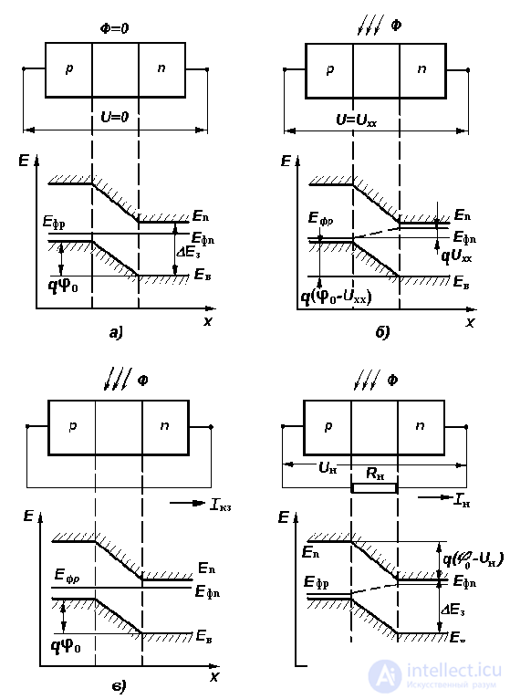
Fig. 3
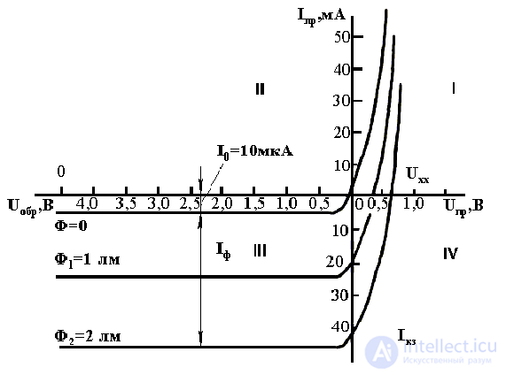
Fig. 4

Comments