
Lecture 22 min.
A charge-coupled device (CCD) is an integrated circuit consisting of a set of MOS (metal-oxide-semiconductor) or MIS (metal-insulator-semiconductor) structures formed on a common semiconductor substrate in such a way that the electrode strips form a linear or matrix regular structure. A particular application of charge-coupled devices is their use as photo-CCDs.
The basis of a CCD is a capacitor with a MOS or MIS structure, capable of storing information packets of charge formed under the action of light. A chain of such capacitors, coupled to one another in a special way, can transfer the charge packets under the action of control voltages from one element of the structure to another up to the output, where the charge packets are converted into a potential or a current.
A
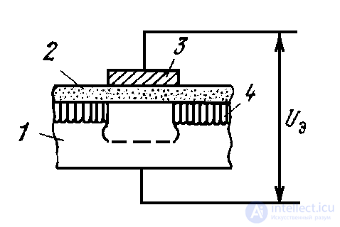
Fig. 1 A cell of the MOS structure: 1-substrate of p-silicon; 2-oxide; 3-conducting electrode; 4-stop-diffusion (SD) region
ctive cell that converts the luminous flux into an electric charge is a capacitor. Fig. 1 shows such a cell, which includes a p-silicon substrate as its base. A layer of oxide is formed on its surface by thermal oxidation, and a conducting electrode is deposited on the oxide. If a positive voltage Ue is applied between the electrode and the substrate, then under the action of the electric field a region depleted of majority carriers will be formed under the conducting electrode - in the case considered, of holes - the stop-diffusion (SD) zone (indicated by dashed lines). Minority charge carriers (here, electrons) accumulate in the resulting potential well. If the charges are produced by photoelectron or thermionic emission, the value of the charge accumulated over a given time turns out to be proportional to the illumination. Fig. 2 shows how the surface potential Us (in relative units) changes as the charge Q accumulates (in relat
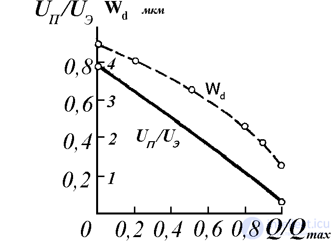
Fig. 2 Accumulation characteristic of a MOS-structure cell
ive units). The same graph shows the dependence of the width d of the depletion layer on the amount of accumulated charge. The nature of the dependence of Us and d on Q is determined by the concentration of the doping impurity and the thickness of the oxide layer. Let us consider the mechanism of charge accumulation in a MOS-structure cell, taking into account the dynamic nature of the potential Ue, for an unilluminated photocell. After a positive potential of sufficiently large amplitude is applied to the metal electrode of the MOS structure, a potential well is formed in the substrate. Owing to thermal generation of minority carriers, charge will accumulate in the cell; depending on the temperature and the properties of the MOS-structure materials, its maximum value is built up over a time from hundredths of a second to several seconds and more. If the value of the charge arising from thermal generation is limited (the so-called logic 0 level), then it is possible to determine the maximum time of accumulation and storage of charge in the cell, i.e. to find the lower limit of the operating frequencies of the storage cell. In real devices at room temperature it is usually set at from a few to tens of kilohertz.
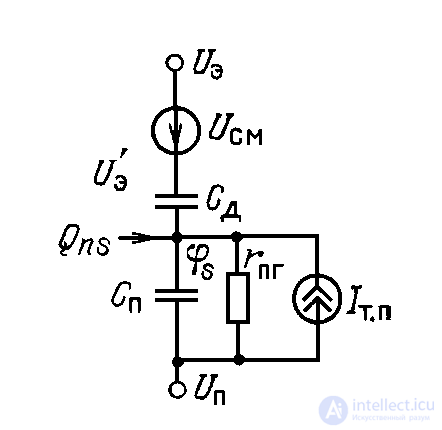
Fig. 3
Electrical model of a memory cell
Fig. 3 shows the equivalent circuit of a memory cell, where: the bias generator Ub represents the influence of the charge built into the dielectric, as well as the potential difference in the structure caused by the difference in work functions of the electrode material (metal) and the semiconductor: Ub = QD/CD - m.s.; Cs is the substrate capacitance; CD is the dielectric capacitance; the current generator It.s represents the thermal-generation surface currents It.s=jt.sSe, where jT.S is the thermal-generation current density at surface states (levels); rleak is the (nonlinear) resistance of charge leakage from the substrate, representing generation in the transition layer; Qns is the maximum charge of mobile carriers corresponding to the equilibrium (steady-state) regime; Qns max = CD(Ue - Uth - Us),

(1)
Where UTH is the threshold voltage of the MIS cell.
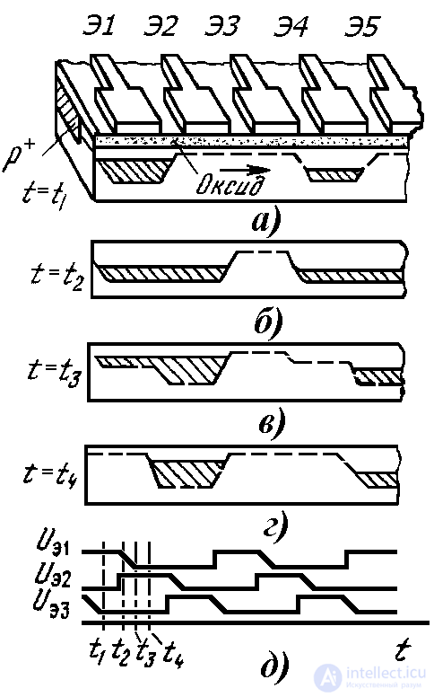
Fig. 4 Linear CCD (a), diagrams for various potentials and various moments of time (b-d) and timing diagrams of potentials (e)
Fig. 4 shows a fragment of a linear CCD made on a common substrate. The distance between the electrodes is so small that, when a positive potential is applied to an electrode, the depletion regions extend practically to the neighboring electrodes. This is conventionally indicated in Fig. 4,b-d, where the dashed line shows the value of the surface potential in the corresponding part of the structure at various moments of time. The same figure shows how the potentials on the electrodes of the structure change with time (Fig. 4, e). The linear array is a three-phase structure in which every third electrode is connected together. As can be seen from Fig. 4, e, the electrode potentials change in a cyclic sequence. The charge packet, which is formed under electrode E1 during the accumulation time, will move under electrode E2 after a positive potential is applied to the neighboring electrode (Fig. 4,b, c). If the potential of electrode E1 is reduced to its initial value, the charge packet will move completely under electrode E2 (Fig. 4,d). Similarly, the charge packet can be shifted under electrode E3, and so on. The cyclic change of the electrode potentials ensures the movement of the charge packets in the direction indicated by the arrow in Fig. 4,a. In this case it is assumed that during the transfer of the charge packets along the structure, the illumination (accumulation) of charges is interrupted.
The structure considered can be used to form the video signal of one line. A picture element (pixel) corresponds to a cell of three elements of the structure. Neighboring charge packets are isolated from each other by the potential barriers of the electrodes held at low voltage.
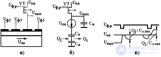
Fig. 5. Readout element:
a - structure; b - electrical model; c - readout signals during charge input and output.
Charges are read out from a memory cell in the following way. A fixed potential U = Uref is set on the sensing electrode (Fig. 5,a), which can be implemented by means of a reset transistor (see Fig. 5,a). After the charges have entered the memory cell, it is switched to the "floating" mode (by disconnecting the electrode from the bias source Ue = 0 Uref 0). The potential well then disappears, and the charge carriers located in it begin to affect the potential of the electrode. The magnitude of the charge that was in the cell is judged from its change.
Uout = Qns/Ce.eq (2)
where Ce.eq is the equivalent capacitance of the memory cell in the readout mode.
Fig. 5.b shows the equivalent circuit of a memory cell using a reset transistor to set the initial voltage before readout, where the capacitance Cl represents the capacitive load of the cell by the subsequent device, Cs is the substrate capacitance, and CD is the dielectric capacitance. Readout at a "floating" electrode makes it possible to determine the amount of charge in the cell under the electrode both when it is transferred under the electrode and when it is removed from under the electrode. In the first case, the reference level (reference voltage) is set without the information charge Qns before the cycle of its input into the cell; in the second, the reference level (reference voltage) is set while the information charge is in the cell, and the magnitude of the charge is judged from the change in the voltage on the electrode (from which the control signal has been removed beforehand) after the charge is taken out of the cell.
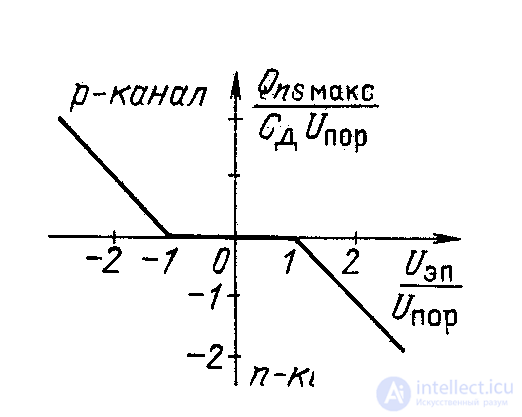
Fig. 6. Dependence of the maximum charge on the amplitude of the control voltage
Fig. 5c shows the timing diagrams of the output voltage for the readout modes when charge Qj is injected and charge Qi is extracted. The potential level UOUT = UREF corresponds to setting the reference level on the electrode of the memory cell, and URST is the voltage controlling the reset transistor. When charge is injected (here, electrons for a cell with an n-channel), the voltage on the electrode decreases (UOUT = Qj/CE.EQ); when charge Qi is extracted, it increases (UOUT = - Qi/CE.EQ>0). When charge is injected into or extracted from a memory cell whose electrode voltage has been preset equal to UREF, the cell passes from one nonstationary state to another, differing in electrode potential by an amount that is practically equal to the change in voltage across the channel–substrate transition layer, i.e., the change in surface potential. The equivalent capacitance CE.EQ = CdCt/(Cd+Ct) + CL is determined (see Fig. 4) practically by the capacitance of the transition layer and the load capacitance, CE.EQ = Ct+CL, since usually Cd>>Ct. The charge is read out of the memory cell, as it were, through the coupling capacitance Cd while residing on the capacitance Ct.
The amplitudes of the control pulses (Fig. 6) applied to the control electrodes (URST, UC ~ 5—20 V).
In real conditions the value of the charge does not remain unchanged as the packet is transferred along the structure. To assess the efficiency of charge packet transfer quantitatively, one uses the efficiency index of charge transfer or loss coefficient (transfer inefficiency) ε = (Qi c - Q(i+1)c)/Qi c, where Qc is the value of the useful charge in the i-th and (i+1)-th cells of the structure. For CCD structures ε = 10-4... 10-5. The frequency dependence of the loss coefficient is shown in Fig. 7. There are special measures for reducing the loss coefficient.
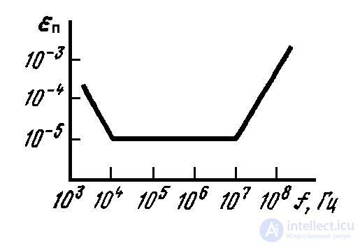
Fig. 7.
Frequency dependence of the loss coefficient
Maximum clock frequency. The speed of CCD structures is limited by the time needed to transfer charge from one storage cell to another. This time reaches a few nanoseconds. Therefore the maximum clock frequencies for CCD structures are tens and hundreds of megahertz (fclock = 10—100 MHz). Thus, these operating ranges of CCD structures ensure their successful use in television systems (TVS) with broadcast-standard parameters.
Maximum and minimum charge packet density (Qn,max ≈ 50 nC/cm2; Qn,min ≈ 50 pC/cm2).
Dynamic range (D = 20 lg Qn,max/Qn,min ≈ 60—80 dB).
Dark current density (Id = 10-10—10-9 A/cm2) Dark current is the result of spontaneous generation of electron-hole pairs. To reduce it, the crystal must be cooled (-40°C).
Noise level. First of all, the source of noise is the light flux itself. That is, the number of photoelectrons accumulated in a cell is determined only to within the square root of their number (Poisson statistics). For example, a charge packet of 10000 electrons will fluctuate from frame to frame with a root-mean-square deviation of 100 electrons. The dark signal is subject to exactly the same statistics, and therefore so is the total (light + dark) signal. For high-quality devices, with low dark current and low transfer inefficiency, the dominant source of noise will be the output device. For modern devices at a frequency of about 100 kHz, an output device noise of 3–6 electrons (with cooling) is considered typical, and in the best devices a figure of 2 electrons is achieved. Since the saturation charge (the maximum size of a charge packet transferred without distortion) is, as a rule, 200–500 thousand electrons, the dynamic range of a CCD reaches approximately 100–110 dB; this is about 18 or 19 bits.
To characterize a PCCD, in addition to the parameters listed above, the spectral range ( Δλ = 0.4—1.1 μm ) and the photosensitivity (Sph = 0.1—0.5 A/W) are specified. It should be noted that the photosensitivity of CCD-based converters is reduced by light absorption in the electrodes (when illuminated from the working side). To weaken this effect, one strives to increase the transparency of the electrodes, as a rule by reducing their thickness (to tens of nanometers). Another method is to etch windows in the electrodes so that the photosensitive regions are open to the incident light. In the latter case, antireflection techniques known from optics, based on depositing thin films, are applied. A variant for reducing unproductive light absorption is to use illumination from the side of the silicon substrate. This method is technologically very complex, because it requires a substantial reduction in the thickness of the substrate (to about 10 μm). All methods of reducing ineffective light absorption lead to an increase in sensitivity in the short-wavelength part of the radiation spectrum.
Maximum and minimum exposures (Hmax ≤ 300 nJ/cm2, Hmin ≥ 300 pJ/cm2), resolution (r = 10—50 lines/mm).
Besides the CCD of the simplest structure (Fig. 4), other varieties have also come into use, in particular devices with overlapping polysilicon electrodes (Fig. 8a), which provide active photoexposure of the entire semiconductor surface and a small gap between electrodes, and devices with asymmetry of near-surface properties (for example, a dielectric layer of variable thickness — Fig. 8b), operating in a two-phase mode. The structure of the buried-channel CCD (Fig. 8c), formed by impurity diffusion, is fundamentally different. Accumulation, storage and transfer of charge take place in the bulk of the semiconductor, where there are fewer recombination centers than at the surface and the carrier mobility is higher. The consequence is an order-of-magnitude increase in fclock and a decrease in the loss coefficient compared with all varieties of surface-channel CCDs.
To perceive color images, one of two methods is used: splitting the optical flux with a prism into red, green and blue, with each of them sensed by a separate PCCD crystal and the pulses from all three crystals mixed into a single video signal; or creating on the surface of the PCCD a film-type stripe or mosaic color-encoding filter forming a raster of multicolored triads.
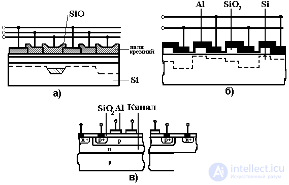
Fig. 8 Varieties of charge-coupled devices with surface
(a, b) and buried (c) channels.
For sensing images in the IR region of the spectrum, three directions are being developed: doping silicon with impurities (In, Ga, Te, etc.) and using the extrinsic photoeffect; developing PCCDs on narrow-gap semiconductor compounds (e.g., on In, Sb for the range λ = 3—5 μm); and creating hybrid structures that combine a photosensitive target, for example on an HgCdTe crystal, with silicon CCD registers that read out the information accumulated in the target.
According to the principle of accumulating and reading out information, PCCDs are divided into linear and matrix types.
In a linear PCCD (Fig. 9, a) the charges accumulated in row 1 during one cycle are transferred to register 2 (from the even elements) and to register 3 (from the odd ones). While along these registers the information is being transferred through output 4 to the signal-combining circuit 5, a new video frame is accumulated in row 1.
In a frame-transfer PCCD (Fig. 9, b) the information sensed by accumulation array 1, is quickly "dumped" into storage array 2, from which it is read out sequentially by CCD register 3; at the same time array 1 accumulates a new frame.
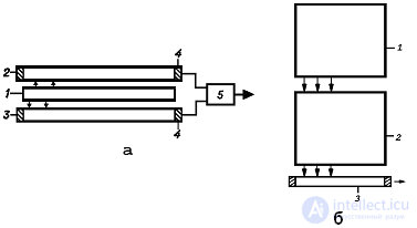
Fig. 9
Accumulation and readout of information in a linear (a) and a matrix (b) PCCD.
Blooming (also spelled "blooming") (from English blooming — halo, smearing of the image) in a CCD is the effect of "spreading" of excess charge from overexposed areas of the CCD array into neighboring cells. The main cause is the limited capacity of the potential well for photoelectrons in a cell. Blooming has a characteristic symmetric shape determined by the geometry of the arrangement of elements on the array. Since about 2006, blooming no longer appears in most consumer devices, because they began to use special antiblooming circuits that drain excess electrons from the cells. However, draining electrons as the potential well fills leads to nonlinearity of the CCD response and complicates measurements. Therefore, for scientific purposes CCDs without antiblooming circuits are still used, and blooming can often be seen, for example, in satellite photographs and in images from interplanetary probes.
Antiblooming is resistance to local overexposure. Because of the surface potential pinning phenomenon, a buried channel cannot be shut off, so as the signal charge in the potential well grows, the channel potential in it decreases, and when it reaches the value of the channel potential under the neighboring electrode, the charge simply begins to spill over this unblocked section of the channel into the neighboring element — and in both directions. In the picture this appears as vertical smearing of bright details of the image. This phenomenon is called optical overexposure (blooming), and while in systems for recording weak signals it can still be tolerated (owing to the low probability of encountering it and the possibility of changing the accumulation time), in cameras for TV it is completely unacceptable.
Blooming is combated by developing a special cell design. The first method (horizontal antiblooming) is that along each column of photosensitive cells a narrow drain region is laid, held at a high positive potential and separated from the potential well accumulating the signal charge by a certain barrier, whose channel potential (sometimes controlled by a separate gate) is higher than the barrier separating the cells from one another. In this case the excess charge will spill over into the drain, and no distortion of the signal in neighboring elements occurs. If a special antiblooming control gate is used, it becomes possible to forcibly clear the charge from the storage cell even without its overflowing, which is nothing other than electronic exposure control.
The price of horizontal antiblooming is some reduction in the fill factor (the drain region cannot contribute to the signal) and an increase in cell size, which is unacceptable for devices with a small cell size. In TV arrays, where the cell size is, as a rule, less than 10 μm, another, very effective method is used to combat blooming — vertical antiblooming. Here the drain region is located not beside but beneath the storage cell, so no increase in cell area is required. The cell here has not just the n+p structure of an ordinary buried channel, but an n+pn– structure, where the middle p-layer serves, as it were, as a "substrate", and the n–-substrate proper serves as the antiblooming drain. With a correct choice of the doping parameters of the layers (and their careful observance during fabrication!), the excess charge from the cell will drain not sideways but downward. The price for this, besides the complex technology, is a strong drop in the IR sensitivity of the device, which is not critical for color television devices.
The variety of CCDs is not exhausted by the types considered above. Thus, CCD line arrays are widely used — both for reading one-dimensional images (for example, barcodes) and in systems with mechanical scanning along one coordinate. The simplest examples are the fax machine and the scanner. Less obvious applications are systems for observing the Earth's surface from spacecraft or aircraft, where the motion of the vehicle itself relative to the Earth is used.
A variety of devices for systems with mechanical scanning are TDI devices — with time delay and integration. Their organization is identical to single-section frame-transfer CCDs, but they differ in the vertical clocking mode: the section is clocked continuously, with the clock frequency chosen so that the speed of movement of the charge pattern equals the speed of movement of the image; each image element then contributes to the same charge packet, which obviously increases the sensitivity of a TDI device compared with ordinary line arrays by a factor equal to the number of rows. TDI devices are the ones widely used in space equipment for observing the Earth's surface. The number of rows in such devices ranges from 64 to 256, and the number of elements horizontally — from 1024 to 4096.
It should be noted that image sensors are not the only application of CCDs. Thus, by adding a device for inputting an electrical signal to a CCD register, one can obtain an analog delay line, in which the delay time is determined both by the number of register elements and by the clock frequency, and therefore can easily be varied. As the element for registering a charge packet one can use not only a floating diffusion but also a floating gate, characterized by nondestructive readout, i.e., one can obtain a register with taps. Such registers are the basis of transversal filters, widely used, for example, in radar signal processing.
A CCD array (charge-coupled device) is one of the types of sensor arrays used in modern video surveillance. It competes closely with CMOS counterparts. The element includes polysilicon artificially separated from the silicon substrate. As the voltage increases, the electric potentials read out by the diodes increase.
In general terms, the system works as follows:
Before shooting begins, all elements are in the same state. There is no spread in the field-strength parameters;
After exposure begins, electrons accumulate that appeared when a light beam hit a particular area. The strength of the light determines how high the resulting voltage will be;
The resulting voltage on each electrode is determined. From it and other parameters one can judge the intensity of the light. When the signal is decoded, the color of the object that entered the frame will also be determined.
Positive features of CCD technology:
A camera based on an element of this type can be used in poorly lit areas and where quality requirements are high.
There are features that limit the range of application of CCD arrays:
As technology advances, the reliability and functionality of these elements increase, so they still remain an alternative worth keeping in mind.
Depending on the field of application and the requirements for parameters, CCDs can be:
Differing in light sensitivity;
Having a full-frame array. This sensor is considered one of the simplest;
With column buffering — charges are read out from top to bottom;
With frame buffering — the number of frames per second is increased;
With orthogonal image transfer, which reduces losses from vibrations and interference;
Differing in size. In the camera specifications it is given in inches.
The array is used in security video surveillance.
With the right choice, it is possible to shoot with good quality in poor lighting and when observing fast-moving objects.

Comments