This circuit shows a Zener diode, a diode that allows current to flow in both the reverse and forward directions.
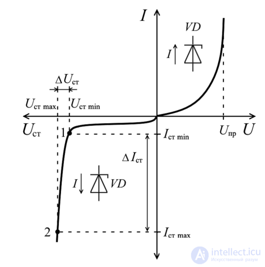
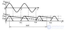
Here the graph in the lower left corner shows voltage versus current.
The current in the forward direction is about 800 mV, and in the reverse direction about -5.6 V.
This page is a utility for simulating график вольт-амперной характеристики стабилитрона online with specified initial values.
Forward bias (anode positive relative to cathode):
Behavior is similar to an ordinary diode.
Current rises sharply at a voltage of ~0.7 V (for silicon Zener diodes).
This mode is rarely used.
Reverse bias (anode negative relative to cathode):
Up to a certain voltage — the reverse current is small.
When the stabilization voltage (Ust) is reached — breakdown occurs.
The current rises sharply, but the voltage remains almost constant — this is the stabilization effect.
Stabilization region:
The voltage across the Zener diode ≈ Ust (for example, 5.6 V).
The current can vary over a wide range, but the voltage remains stable.
This region is used in voltage stabilization circuits.
On the graph:
X axis — voltage (V)
Y axis — current (mA)
In the lower left quadrant — reverse breakdown and stabilization
In the upper right — forward bias
The main difference between a Zener diode and an ordinary diode lies in its ability to operate in reverse breakdown mode for voltage stabilization.
Here is a brief comparison:
| Characteristic | Ordinary diode | Zener diode |
|---|---|---|
| Reverse voltage | Not allowed — leads to breakdown | Allowed — used for operation |
| Purpose | Passing current in one direction | Voltage stabilization |
| Operating mode | Forward bias | Reverse bias |
| Type of breakdown | Destructive | Controlled, stable |
| Application | Rectification, protection | Voltage regulators, reference voltages |
In essence: An ordinary diode blocks current in the reverse direction, whereas a Zener diode, on the contrary, is designed to operate in the reverse direction, where upon reaching a certain voltage (the stabilization voltage) it begins to conduct current, holding the voltage almost constant.
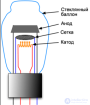
The typical Zener diode connection circuit is a voltage stabilization circuit in which the Zener diode operates in reverse breakdown mode. Here is how it looks and works:
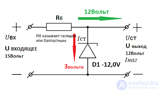
Power source — a constant voltage, slightly higher than the stabilization voltage.
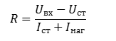
Resistor (current-limiting) — connected in series, limits the current through the Zener diode.
Zener diode — connected in reverse bias (cathode to plus, anode to minus).
Load — can be connected in parallel with the Zener diode.
The source supplies a voltage higher than the stabilization voltage of the Zener diode.
The resistor reduces the current to a safe level.
The Zener diode enters breakdown mode and holds the voltage across the load constant — equal to U<sub>st</sub>.
When the input voltage or current changes, the Zener diode compensates for this, maintaining a stable output voltage.
Uin — input voltage
Ust — stabilization voltage
Ist — Zener diode current (usually 5–20 mA)
Iload — load current
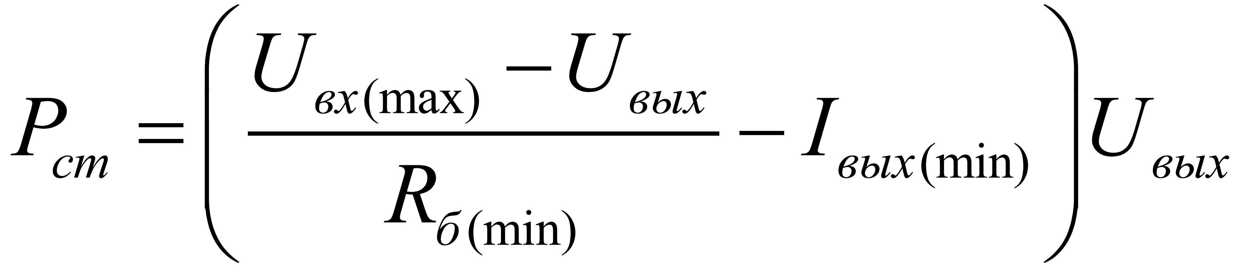
The power dissipation of a Zener diode Pst characterizes its ability not to overheat above a certain temperature over a long period of time. The higher the value of Pst, the more heat the semiconductor device is able to dissipate.
Power dissipation is calculated for the most unfavorable operating conditions of the device, so the maximum possible operating Uin and the smallest values of Rb and Iload are substituted into the formula below:


Comments